Researchers in the Electronic + Magnetic Materials + Devices Group (Argonne National Laboratory) and at Politecnico di Milano in Italy explored the limits of antiferromagnetism in a nanostructured material for the first time, measuring the temperature required to support antiferromagnetic order in atomic monolayers of manganese on tungsten as the dimensions of the structures are reduced.
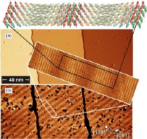 (Top) Schematic of the spin structure of the Mn monolayer on W(110) (6-nm repeat structure). (a) Topography and (b) differential conductance at 40 K. (Inset) High-resolution topographic data taken with a spin-sensitive tip; stripe contrast is related to the degree of antiferromagnetic order.
While these boundaries are well understood in ferromagnetic materials, antiferromagnetic materials - where neighboring magnetic moments cancel rather than add together - have proven more challenging to unravel.
This study exploits the unique properties of manganese spin spirals on tungsten to correlate spin-sensitive scanning tunneling microscopy techniques on the atomic scale with electronic signatures, showing that the ordering temperature for the antiferromagnetic structure depends both on its size and its orientation with respect to the crystal lattice.
Such investigations will help guide the way to next generation platforms for ultra-high-density data storage and novel sensing capabilities.
More information: Paolo Sessi, Nathan P. Guisinger, Jeffrey R. Guest, and Matthias Bode, Phys. Rev. Lett. (in press)