Mar 9 2020
A research team from Sungkyunkwan University based in South Korea has given a detailed review of heterogeneously integrated two dimensional (2D) materials in a study published in the NANO journal.
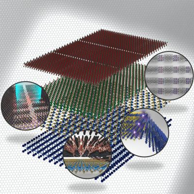 Schematic illustration of the newly emerged 2D heterostructures research with various heterogeneous integration of 2D materials. Image Credit: World Scientific.
These materials belong to a large library of atomic 2D materials that have selectable material characteristics to unlock interesting possibilities for the development of new functional devices.
Ever since graphene was discovered by Andre Geim and Konstantin Novoselov, 2D materials like black phosphorous (BP), graphene, hexagonal boron nitride (h-BN), and transition metal dichalcogenides (TMDCs) have attracted a great deal of attention because of their extensive physical properties as well their broad range of applications in optoelectronic and electronic devices.
The study on these 2D materials has advanced to the point, where a comprehensive library of atomically thin 2D materials with selectable material characteristics has been made and remains growing.
By stacking or integrating these 2D materials, 2D heterostructures can be constructed, which are made by directly stacking separate monolayers containing a variety of materials. Within a 2D heterostructure, each monolayer is very stable that can be attributed to the powerful covalent bonds that exist between the atoms inside that monolayer.
But the forces that exist between the monolayers, maintain the mentioned monolayers placed one above the other to create the 2D heterostructure. The said forces happen to be comparatively weak van der Waals interactions. Hence, every monolayer maintains its inherent properties.
In traditional semiconductor heterostructures, the component material selection is limited to those having analogous lattice structures. But in stacked heterostructures, the lattice mismatch requirements can be relaxed because of the weakness of the van der Waal’s forces. This implies that semiconducting, metallic, or insulating 2D materials can be combined to create a single 2D heterostructure despite their varied lattice structures.
When a monolayer is stacked along with the other monolayers produced from different materials, a new range of heterostructures with atomically thin 2D heterojunctions can be developed.
Heterostructures produced from a specific combination of materials will exhibit some specific physical properties based on the type of materials they are produced from. The strange physical properties of 2D heterostructures make them well-suited for use in an extensive range of applications.
In this study, numerous 2D heterostructures are discussed along with a description of innovative optoelectronic and electronic properties, sophisticated synthesis technical developments, and the available new functional applications. This study gives a better understanding of the present research trends in 2D materials to investigate future opportunities for nanomaterial studies.
The study was financially supported by the National Research Foundation of Korea funded by the Korean government (grant nos. 2013M3A6B1078873, 2015R1D1A1A09057297, 2017R1A4A1015400, and 2017R1A2A2A05001403).
The study’s corresponding authors are Euyheon Hwang ([email protected]) and Sungjoo Lee ([email protected]) from SKKU Advanced Institute of Nanotechnology and Department of NanoEngineering, Sungkyunkwan University.
Source: https://www.worldscientific.com/