The development of a high-conductivity material by a team of researchers in China could significantly lower contact resistance and Schottky barrier height in crucial areas of electronic and optoelectronic microchips, opening the door for computer and digital imaging parts that use less power in relation to their performance than current chipsets.
The Bi2Te3 nanosheets with high conductivity were grown on MoS2 as van der Waals contacts, leading to a high-performance MoS2 FET. Image Credit: Nano Research, Tsinghua University Press
Molybdenum disulfide (MoS2) is a material that is so thin it is categorized as two-dimensional. In other words, the material is grown in sheets that extend in the X and Y directions but are essentially immeasurable on the Z axis because the material is frequently only one molecule or atom tall.
On December 5th, 2022, the team at Hunan University’s College of Materials Science and Engineering, led by professors Dong Li and Anlian Pan, published its findings in the journal Nano Research.
The authors of the study “Epitaxial van der Waals Contacts for Low Schottky Barrier MoS2 Field Effect Transistors” highlight how 2D materials have drawn a lot of interest due to their numerous and tunable electronic states and a variety of optical, electronic, and mechanical properties.
These qualities make them promising building blocks for upcoming high-performance electronic and optoelectronic devices, such as transistors, photodetectors, and light-emitting diodes.
The performance of a 2D semiconductor transistor mainly relies on the microscopic connections among components within a chip, and the quality of those connections depends ultimately on the material used in these contact points, which are always metals achieved by thermal evaporation, limiting the performance of 2D materials-based transistors.
Dong Li, Professor, College of Materials Science and Engineering, Hunan University
Li’s team combined semiconducting MoS2 with the highly conductive metalloid and semimetal Bismuth Telluride (Bi2Te3) to create a better-performing contact point. The hybrid growth of these metalloid nanosheet crystals showed initially promising results.
Li further stated, “Attempts in recent years to achieve epitaxially grown semiconductor contacts have succeeded in laboratory settings, but weren’t likely candidates for being scaled up to the level that would be needed to manufacture chips and other devices.”
“Most of these methods put forward strict requirements for material preparation and strict fabrication and are hardly compatible with further manufacturing processes in integrated circuits. The realization of high-quality semiconducting 2D materials and excellent contact at the same time is critical for reliable device applications,” he continued.
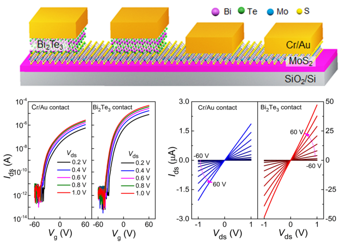
Vertical stacking of MoS2 and Bi2Te3 in a two-step synthesis procedure was required to create this experimental van der Waals contact.
A piece of silicon dioxide (SiO2) substrate was positioned downstream of a quartz tube, and molybdenum trioxide (MoO3) and sulfur powder were added to the center and upper streams of the furnace, respectively, to serve as the growth medium for the monolayer of MoS2.
Bi2Te3 powder and MoS2 nanosheets that had already grown were positioned in the center and at the base of the quartz tube, respectively, for the second step growth of the Bi2Te3 nanosheet.
MoS2/Bi2Te3 heterostructures were produced following a 5-minute growth period. Bi2Te3 nanosheet thickness and nucleation sites may be affected by the growth temperature and gas flow rate, according to the study’s findings.
The team used a variety of electrical and imaging techniques to examine the appearance and conductive performance of the hybrid nanosheets, and they discovered that the new contact method performed significantly better than gold contacts, which are useful as a baseline measurement because gold is so frequently used in chip manufacturing.
A crucial step toward making the MoS2/Bi2Te3 semiconducting contact method a strong candidate for future commercial viability, the new contact method was tested at various ambient temperatures and maintained good performance at room temperature.
Li stated, “Combining the multiple advantages, the epitaxial van der Waals Bi2Te3 contacts provide a new strategy for the application of 2D MoS2 in future optoelectronic devices. Now that we have established the functionality of Bi2Te3 contacts in a controlled laboratory setting, the next steps will be to continue to investigate and optimize this method, with the hope that this new technology can eventually be adopted for widespread use in more powerful, lower energy consumption electronics.”
Journal Reference
Liu, H., et al. (2022) Epitaxial van der Waals contacts for low schottky barrier MoS2 field effect transistors. Nano Research. doi:10.1007/s12274-022-5229-y.
Source: http://www.tup.tsinghua.edu.cn/en/index.html