Instrumented indentation, or nanoindentation, is an important technique used for measuring the mechanical properties of materials, and can be conducted in situ even on the circuit board itself.
This technique can be used under a wide range of circumstances. For instance, mechanical properties can be determined at room temperature, or higher temperatures, after a certain number of thermal cycles.
This article demonstrates the use of instrumented indentation to quantify the in-situ Young’s modulus and strain-rate sensitivity of a standard lead-free solder alloy called SAC 105, which is mainly composed of tin alloyed with 0.5% copper and 1% silver.
Strain-Rate Sensitivity of Solder Alloy
Since SAC 105 contains 98.5% tin, it is useful to compare the results to those determined by others for unalloyed tin. The nominal Young’s modulus of tin is 50GPa. Recently, Burek et al. calculated the tin’s strain-rate sensitivity by compressing nanoscale pillars produced by electron-beam lithography.
Although the yield stress depends on the diameter of the pillar, strain-rate sensitivity does not. For pillars with a diameter of 560 and 920nm, a strain-rate sensitivity of 0.181 was reported.
Instrumented Indentation Test vs. Traditional Hardness Tests
Instrumented indentation testing is a development of conventional hardness tests such as Rockwell, Brinell, Knoop, and Vickers. This testing is similar to standard hardness testing in that a hard indenter is made to contact with the test material.
Conventional hardness testing however produces just one measure of deformation at a single applied force, whilst during an instrumented indentation test, both force and penetration are determined for the entire time that the indenter remains in contact with the test material.
In 1992 an analytical method was proposed by Oliver and Pharr, with which contact area can be determined from the force-displacement data, thus removing the necessity to image the residual impression when measuring hardness (H) as the indentation force separated by the contact area.
Moreover, the displacement retained as the indenter is withdrawn shows elastic recovery, and hence can be utilized to acquire Young’s modulus (E). To this end, superimposing a small oscillation on the indentation force enables the separation of plastic and elastic components of deformation, and the useful benefits of this separation are numerous.
Instrumented indentation is specifically suitable for testing small volumes of material such as particles, thin films, etc. Nevertheless, this technique is also used for larger volumes of material, thanks to its speed and simplicity. Additionally, sample preparation is quite easy and a number of tests can be carried out on a single sample.
Besides hardness and Young’s modulus, this instrumented indentation technique can be utilized to characterize creep in metals, because hardness is a sign of the metal’s yield stress (σ).
Under creep conditions, the yield stress relies on strain rate and temperature. As a manifestation of yield stress, hardness relies on strain rate and temperature just as yield stress does.
Vacancies diffuse into the material and allow dislocations to pass more freely and surmount obstacles to motion. Therefore, the relationship between strain rate (ε) and stress (σ) can be captured with an Arrhenius term multiplied by stress raised to an exponent.
Experimental Framework
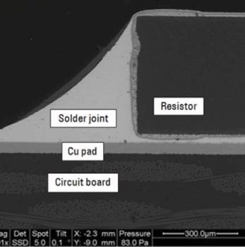
Figure 1. On-board SAC 105 solder joint.
In this study, a sectioned solder joint was tested which was formed between a 2512 chip resistor held in an epoxy potting compound and a printed wiring board (PWB) (Figure 1). The core metallization was copper and the board was coated with Organic Solderability Preservative.
The solder paste was SAC 105 (98.5%wt tin, 0.5%wt copper and 1%wt silver). The reflow was performed in air; the time above liquidus was 50 to 74 sec and the reflow temperature was 244ºC. The ramp-down rate was 3.41°C/sec and the ramp-up rate was 0.48°C/sec. After reflow, the board was aged at 150°C for 24 hours.
For all testing procedures, a KLA Nano Indenter G200 equipped with an XP head and a Berkovich indenter was utilized. The Continuous Stiffness Measurement (CSM) option was used to calculate the elastic contact stiffness by oscillating the indenter.
“G-Series XP CSM Thin Film SRS” is a test method, which imposes a user-defined strain rate and returns the hardness for that rate. This method was used for all testing. It is mainly suitable for testing at slow strain rates as it is not sensitive to thermal drift. The insensitivity to drift is obtained by means of measuring displacement and contact area.
This is valid as long as the Young’s modulus of the material is not dependent on strain rate, which is a good assumption for metals. All properties were determined at 1000nm (1μm) indentation depth.
Six indentations were carried out at 0.05/sec, 0.01/sec, and 0.002/sec. Then, the CSM option was utilized to oscillate the indenter at 45Hz with 2nm amplitude. All tests were performed at 29.15+0.10°C temperature.
Results and Discussion
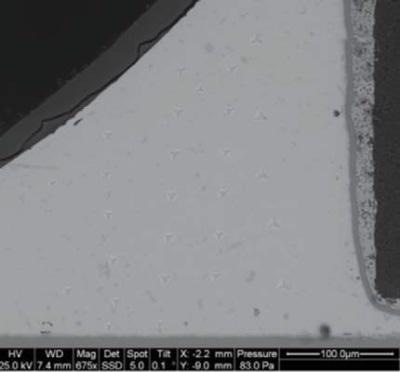
Figure 2. Residual impressions from indentation testing on SAC 105 solder joint.
Table 1. Summary of indentation results for SAC 105 at various strain rates.
| Indent |
Strain Rate 1/s |
E GPa |
H GPa |
| 1 |
0.002 |
|
0.1058 |
| 2 |
0.002 |
|
0.1105 |
| 3 |
0.002 |
|
0.1357 |
| 4 |
0.002 |
|
0.1915 |
| 5 |
0.002 |
|
0.1444 |
| 6 |
0.002 |
|
0.1049 |
| 7 |
0.01 |
|
0.1871 |
| 8 |
0.01 |
|
0.1770 |
| 9 |
0.01 |
|
0.1744 |
| 10 |
0.01 |
|
0.2026 |
| 11 |
0.01 |
|
0.2041 |
| 12 |
0.01 |
|
0.1929 |
| 13 |
0.05 |
50.81 |
0.2491 |
| 14 |
0.05 |
48.20 |
0.2292 |
| 15 |
0.05 |
51.70 |
0.2339 |
| 16 |
0.05 |
49.01 |
0.2089 |
The residual indentation impressions on the SAC 105 solder joint is shown in Figure 2. Impressions from initial tests can also be seen. Table 1 shows the results for all successful tests.
Due to an unexpected degree of surface roughness, two tests at the highest strain rate failed. When surface roughness is expected, it is accommodated by means of a larger approach distance.
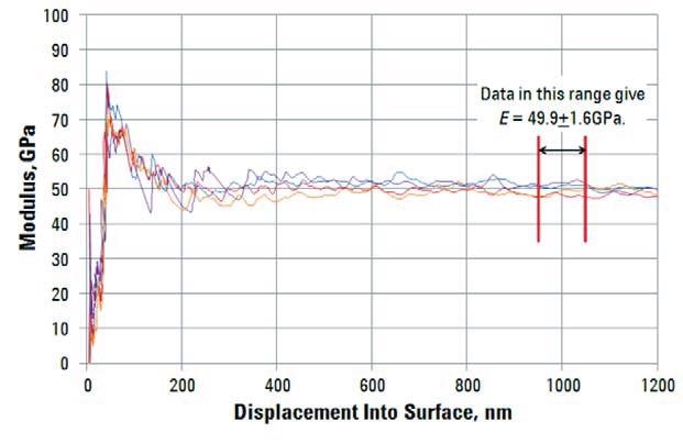
Figure 3. Young’s modulus as a function of indenter displacement for indentation tests at the highest strain rate (0.05/sec).
Figure 3 illustrates the Young’s modulus as a virtue of penetration depth for tests at the highest strain rate of 0.05/sec. Also, anomalous values at small displacements may be due to the presence of an oxide layer.
Nevertheless, Young’s modulus is approximately 50GPa once the indenter displacement surpasses 200nm, and the quoted value (49.9±1.6GPa) is achieved from the displacement range identified in Figure 3. This measured value compares extremely well with the nominal Young’s modulus for tin, which is 50GPa. Hence, for SAC 105, the alloying elements of copper and silver do not significantly influence the Young’s modulus.
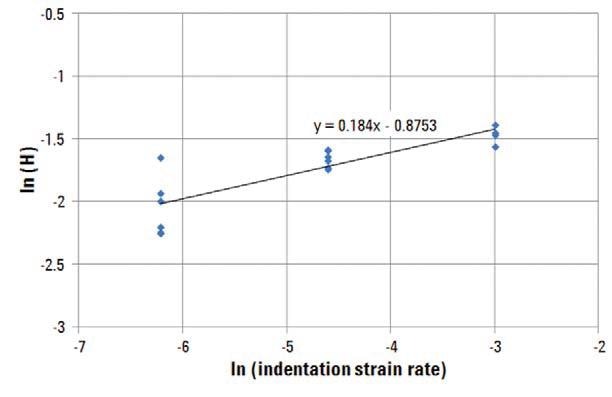
Figure 4. Natural logarithm of hardness vs. natural logarithm of strain rate; the slope of these data give a strain-rate sensitivity of m = 0.184±0.013.
Figure 4 outlines the linear fit to the ln(H) vs. ln (εi) results for all 16 successful indentations. The slope of this line is 0.184 and the typical error of the slope is 0.013, providing a strain-rate sensitivity of m = 0.184±0.013. The related stress-exponent for creep is n = 5.43. These values compare extremely well with those calculated by Burek et al. for bulk tin (cf. m = 0.181, n = 5.54) [2].
Therefore, it appears that for SAC 105, the alloying elements do not significantly influence strain-rate sensitivity either.
The CSM option is an important tool for precise measurement of the Young’s modulus of soft metals. This type of dynamic measurement entirely deconvolutes the plastic and elastic deformation, thus enabling the precise characterization of elasticity.
Moreover, with a continuous measurement of Young’s modulus, different phenomena such as substrate influence and surface anomalies can be distinguished.
Conclusion
Instrumented indentation was used to quantify the Young’s modulus and strain-rate sensitivity of the SAC 105 solder alloy. At room temperature, the strain-rate sensitivity was m = 0.184±0.013 and the Young’s modulus was E = 49.9±1.6GPa.
These values are extraordinarily close to what others have quantified for unalloyed tin through compression and uniaxial tension experiments, thus lending credibility to the usefulness of the instrumented indentation technique.

This information has been sourced, reviewed and adapted from materials provided by KLA Corporation.
For more information on this source, please visit KLA Corporation.