KLA Instruments™, a division of KLA Corporation, has expanded its defect inspection and metrology portfolio in 2023 to include new systems for semiconductor process development and control, including the Filmetrics® R54-300 sheet resistance mapping system, the F54-XYT-300 and F60-c film thickness mapping systems, and the Nano Indenter® G200X with the Semiconductor Pack.
The R54-300 brings 300mm wafer handling capability to benchtop sheet resistance mapping and can be configured for either four-point probe (4PP) or eddy current (EC) measurement techniques. The R54-300 delivers process optimization metrology in a compact, high-performance benchtop package with easy-to-use software.
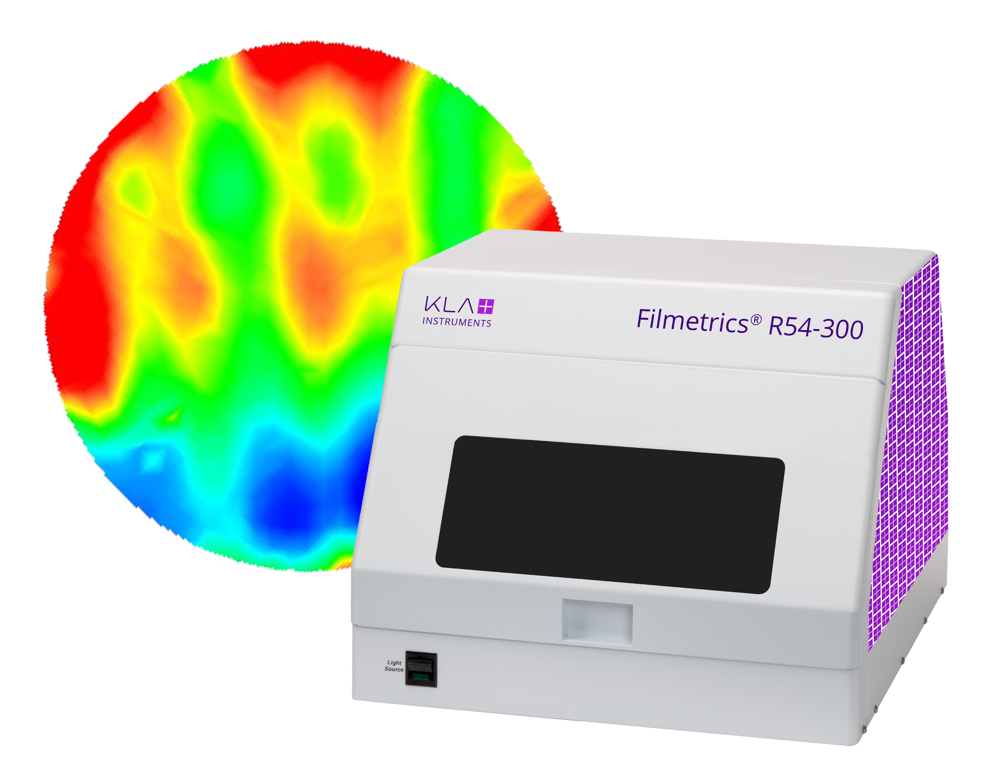
The Filmetrics® R54-300 from KLA Instruments delivers 300mm wafer sheet resistance mapping using either four-point probe (4PP) or eddy current (EC) measurement techniques. Image Credit: KLA Instruments
The F54-XYT-300, shown in the video below, is the newest iteration of the Filmetrics line of film thickness mapping systems, offering pattern recognition and flexible configurations that measure a variety of film thickness ranges. The fully automated F60-c, also shown in the next video, includes a wafer handler for fast measurement of unpatterned films. Both systems use the standard FILMapper software platform with predefined or customizable map patterns to enable wafer mapping in minutes.
F54-XY_23s
The Filmetrics® F54-XYT-300 from KLA Instruments measures film thickness for patterned or unpatterned wafers up to 300mm round.
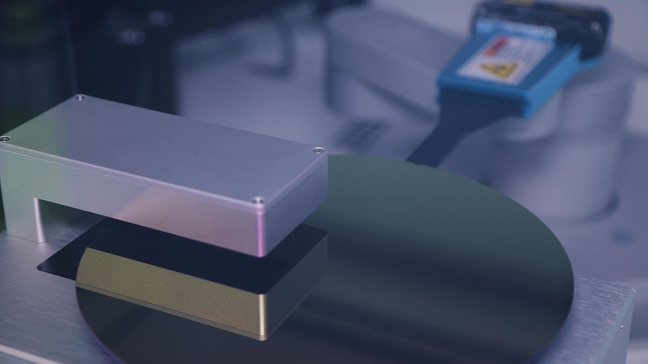
The re-engineered F60-c combines Filmetrics film thickness mapping technology with the improved automation of KLA Instruments™ production metrology systems. Image Credit: KLA Instruments
The Nano Indenter G200X system is optimized for mapping mechanical properties of bulk materials, films and more. The G200X Semi Pack option is a high-performance hardware and software package specifically designed for semiconductor and compound semiconductor applications. The Semi Pack provides the best-known methods for nanomechanical evaluation of films, surfaces and interfaces to evaluate adhesion and brittleness to minimize latent defects. This new information can be used to create an engineering feedback loop to produce stronger material systems and increase device yield and reliability.
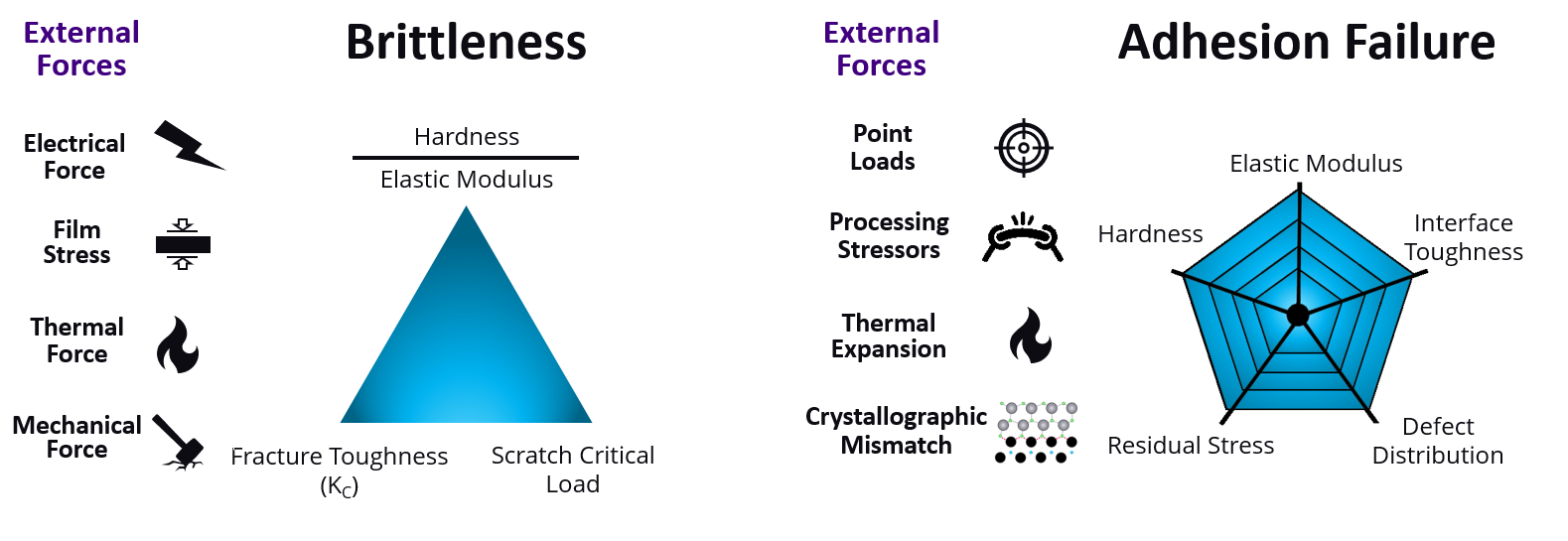
The Nano Indenter® G200X characterizes various nanomechanical properties to characterize factors contributing to brittleness and adhesion failure. This information helps to identify sources of latent defects early in the manufacturing process to minimize expensive device failures in later use. Image Credit: KLA Instruments
Come visit us at Semicon Europa Booth B1341 to meet our team and learn about KLA Instruments defect inspection and metrology solutions for your semiconductor and compound semiconductor applications.
KLA Instruments offers a portfolio of profilometers, nanoindenters, thin film reflectometers, sheet resistance mappers and specialized defect inspection systems. For industry experts, academics and other innovators, we deliver trusted measurements, enabling the world’s breakthrough technologies.