The Zeta™-20 benchtop optical profiler is a non-contact 3D microscope and surface topography measurement system.
This 3D optical profiling system has been powered by patented ZDot™ technology and Multi-Mode optics, allowing measurement of a range of samples: transparent and opaque, smooth to rough texture, low to high reflectance, and step heights ranging from nanometers to millimeters.
The Zeta-20 3D optical profiling system combines six optical metrology technologies in one configurable and user-friendly system. ZDot measurement mode concurrently gathers a high-resolution 3D scan and a True Color infinite focus image.
Other 3D measurement methods include Nomarski interference contrast microscopy, white light interferometry, and shearing interferometry. Film thickness could be quantified with ZDot or a combined broadband reflectometer.
The Zeta-20 is a high-end microscope for sample review or automated defect inspection. The Zeta-20 3D optical profiling microscope assists R&D and production environments by offering extensive roughness, step height, film thickness measurements, and defect inspection capability.
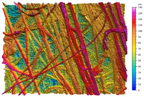
N95 mask fiber topography measured by the Zeta-20. Image credit: KLA Instruments™
Copper laser via topography measured by the Zeta-20. Image credit: KLA Instruments™
Key Features
- User-friendly optical profiler with ZDot and Multi-Mode optics to fulfill an extensive range of applications
- High-quality microscope available for sample review or defect inspection
- ZDot: concurrently gathers a high-resolution 3D scan and a True Color infinite focus image
- ZXI: White light interferometry for extensive area measurements with high z resolution
- ZIC: Interference contrast for quantitative 3D data of surfaces with sub-nanometer roughness
- ZSI: Shearing interferometry for images available with high z resolution
- ZFT: Film thickness and reflectance are quantified with a combined broadband reflectometer
- AOI: Automatic optical inspection to measure defects on the sample
- Production capability: completely automated measurements with sequencing and pattern recognition
Image Credit: KLA Instruments™
Applications
- Surface topgraphy: visualize and measure surface features in 3D
- Step height: 3D step height from nanometers to millimeters
- Stress: 2D thin film stress
- Form: 3D bow and shape
- Texture: 3D roughness and waviness on smooth to highly rough surfaces
- Film thickness: transparent film thickness ranges from 30nm to 100µm
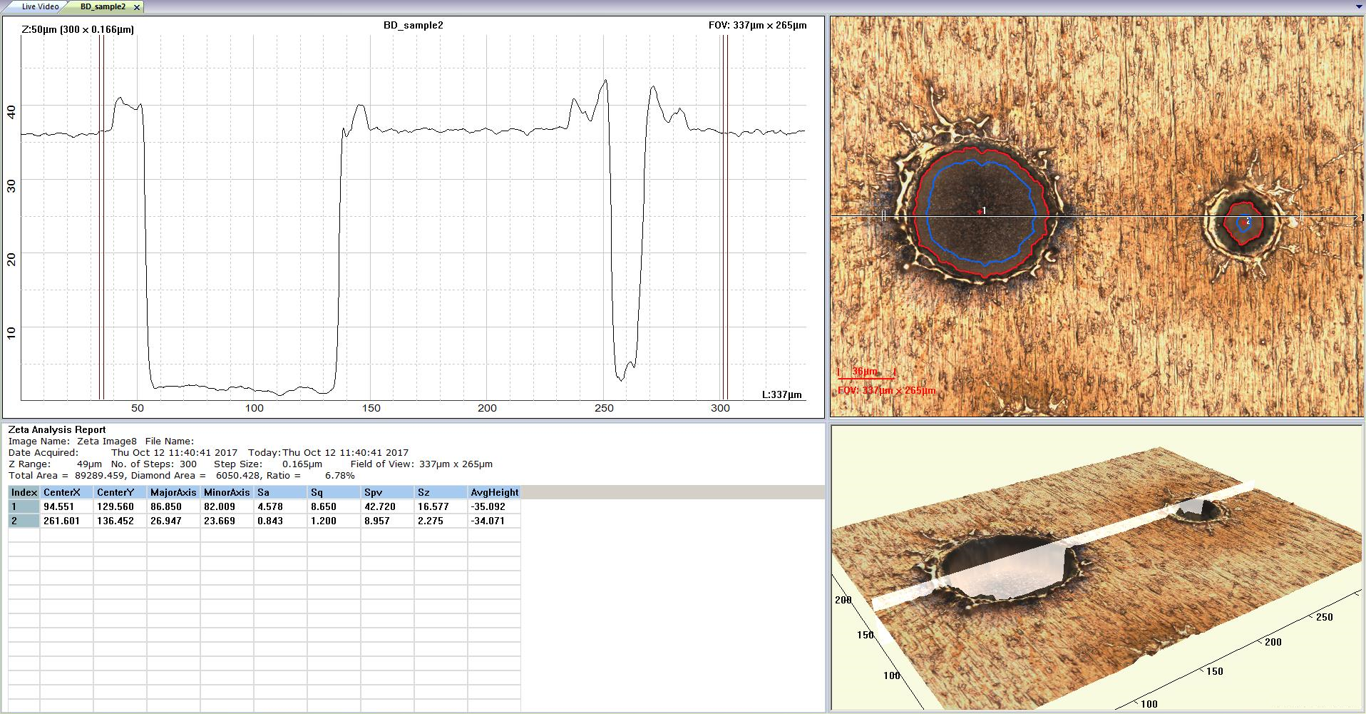
- Defect inspection: capture defects greater compared to 1µm
- Defect review: KLARF files may be utilized to navigate to defects to quantify 3D surface topography or scribe defect locations
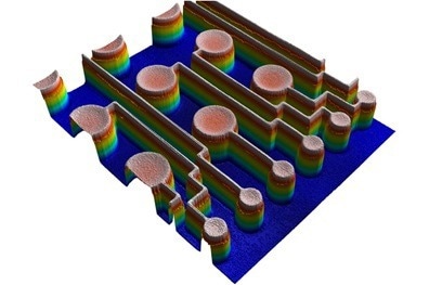
Image Credit: KLA Instruments™
Industries
- Solar: photovoltaic solar cells
- Semiconductor and compound semiconductor
- Data storage
- Semiconductor WLCSP (wafer-level chip scale packaging)
- Semiconductor FOWLP (fan-out wafer-level packaging)
- PCB (printed circuit board) and adaptable PCB
- MEMS: Micro-electro-mechanical systems
- Medical devices and microfluidic devices are provided
- Universities, research labs, and institutes
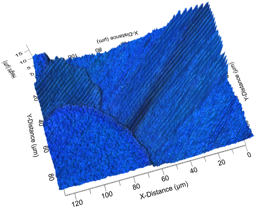
Image Credit: KLA Instruments™