Introduction
The consistency of soldered connections in electronic packaging relies on mechanical integrity, which in turn depends on mechanical properties. In this article, an advanced form of nanoindentation is used to quickly and quantitatively map the mechanical properties of all parts of a solder joint, with a particular focus on the SAC 305 solder alloy (96.5% tin, 3% silver, and 0.5% copper) due to its extensive usage in electronic packaging.
Solder Joints
In general, solder joints exhibit a complex microstructure that depends on a number of factors such as the size of the joint, the plating and solder materials, and the exposure of the joint to temperature and stress over time. The development of intermetallic compounds within a tin-rich matrix is favored by certain alloys.
In case of soldered joints, the development of intermetallic compounds depends on the metallization utilized to make components for bonding. Copper is usually employed for board and electronic terminals. A nickel layer is typically applied to the copper, followed by a gold layer that improves wetting and protects the nickel. When such terminals are linked by the SAC 305 solder, large amount of AuSn4 is formed that travels to the solder joint interface over time to form a fragile layer.
Recently, Mukherjeeet al. demonstrated that the transfer of AuSn4 to the solder joint interface can be prevented by substituting the nickel and gold metallization with a tin layer over the copper, even when gold is available from metallization on the mating surface.
Instrumented Indentation
Instrumented indentation, also known as nanoindentation, is a highly localized technique that is suitable for quantifying the mechanical properties of soldered connections. This method demands minimal sample preparation and is similar to standard hardness testing. It involves pressing a hard indenter, usually a diamond, into a test surface while constantly monitoring the penetration and contact force; Young’s modulus and hardness are measured from each indentation.
In this study, an advanced form of nanoindentation called Express test is used. This test optimizes both the indentation process and data handling to enable rapid testing. When Express Test is used, the tip of the indenter hovers just above the surface and conducts indents in quick succession to form a series of discrete indentations.
Experimental Procedure
Soldered connection was made to promote the development of intermetallic compounds. For sample preparation, different bonding preparations were used for two mating copper platens. The first copper surface was coated with 2.54µm of nickel, followed by 3.81µm of silver, and the second copper surface was coated with 1.27µm of tin. The plated copper surfaces were then coupled using the SAC 305 solder alloy. After soldering, the joint was aged for a month at 121°C. Previous work on this sample has demonstrated that (Cu, Au)6Sn5 develops at the interface with tin metallization and AuSn4 develops in the bulk of the joint.
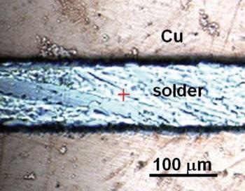
Figure 1. SAC 305 solder joining two copper platens.
In order to prepare the joint for nanoindentation, the sample was placed in epoxy and ground with silicon carbide paper, and was then polished using alumina suspensions. An optical image of the joint, prepared for nanoindentation is shown in Figure 1.
All testing was carried with a KLA NanoIndenter G200 using NanoVision, Express Test, and an XP head equipped with a Berkovich indenter. The test method “Express Test to a Force” was used to conduct two indentation arrays. The first array included 40 x 40 indents within a 100µm x 100µm area and covered the breadth of the solder joint, whilst the second array was 40 x 20 indents within a 100µm x 50µm area and covered the interface between the copper platen and solder with tin metallization. All indentations were carried out to a peak force of 2mN.
Results and Discussion
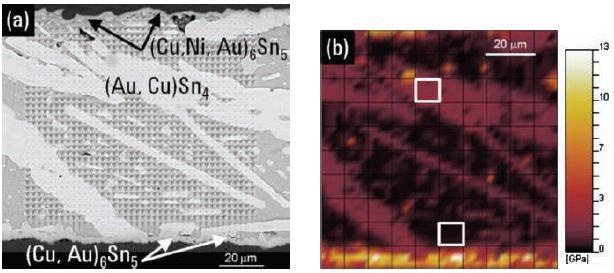
Figure 2. (a) Indentation array on a SAC 305 solder joining two copper platens, and (b) resultant hardness map.
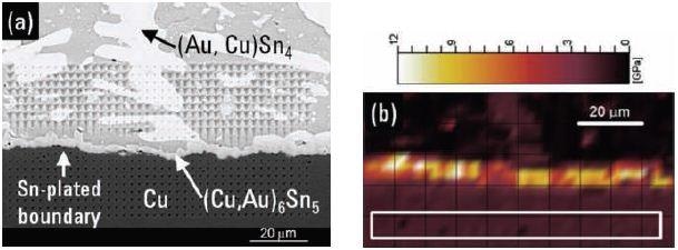
Figure 3. (a) Indentation array on a SAC 305 solder and Sn-plated Cu platen, and (b) resultant hardness map.
Figures 2 and 3 depict the side-by-side images of the indentation arrays and the ensuing hardness maps. The time taken to make the large array was 68 minutes, but without Express Test, this would have taken more than a day.
The various materials in the joint are differentiated in proportion to hardness. To report quantitative hardness values for each type of material, domains were chosen that were clearly within one type of material. Table 1 summarizes the quantitative hardness values.
Table 1. Hardness of SAC 305 solder-joint constituents.
| Material |
Hardness (GPa) |
| Sn-rich matrix |
0.51±0.07 (N = 16) |
| AuSn4 |
2.12±0.18 (N = 16) |
| (Cu, Au) 6Sn5 |
> 8 |
| Cu platen |
2.01±0.10 (N = 100) |
With a hardness of about 0.5GPa, the bulk solder is the softest material. The intermetallic AuSn4 that forms in the bulk has a hardness of approximately 2GPa, which is analogous to that of copper. The (Cu, Au)6Sn5 that forms at the tin-plated platen has a hardness of more than 8GPa. This difference in hardness is a concern for reliability as this means that plastic strains induce much higher stresses in the intermetallic compound than in the surrounding material, thus causing a discontinuity in stress at the boundary. Such a discontinuity boosts the local stress-intensity factor, which drives fracture.
Conclusion
Since electronic reliability relies on mechanical integrity, the aim of this work was to use nanoindentation to map the mechanical properties of the SAC 305 solder joint. However, using conventional nanoindentation for such quantitative mapping would have taken significant amount of time. Using the Express Test option for KLA's NanoIndenter G200, quantitative and highly resolved hardness maps were produced in just an hour.

This information has been sourced, reviewed and adapted from materials provided by KLA Corporation.
For more information on this source, please visit KLA Corporation.