Lasers are being utilized for surface conditioning and precision micro-scale machining in a wide range of industries, including bio-medical device, LED, and semiconductors manufacturing. However laser ablation processes create surfaces that pose a major problem to traditional profilers, due to high aspect ratios, fluctuating geometry, high roughness, etc. This article discusses some of these issues and demonstrates how surfaces can be quantified using the Zeta-20 optical profilers in true color, regardless of their material, roughness, or size.
Industry Challenges
The following factors are required for successful application of laser induced surface topography:
- Different types of materials
- Non-destructive testing
- Precise data
- High aspect ratio measurement
- Speed
- Convenience
- Cost Savings
- Actionable and quantifiable data
The Zeta-20 Optical Profiler Advantage
The Zeta-20 Optical Profiler offers the following benefits:
- Non-contact optical profiler
- Sample preparation is not required
- Fully automated
- Rapid scan time
- Easy-to-use graphical user interface
- Coated, transparent, and opaque samples
- Unique algorithm and highly efficient illuminator
- True color and broad band, without coherent artifacts
- Automated height, critical dimension (CD), and volume reporting (Figure 1)
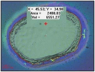
Figure 1. Critical dimension and volume quantification with true color.
Technology
In 2009 the very first optical profiler was designed based on confocal grid structured illumination (CGSI) technology. This method evolved confocal microscopy, allowing complex surfaces to be measured and enabling true color imaging. The patented ZDot™ (CGSI) imaging technology by Zeta provides a suitable solution for laser cutting applications, because it does not have the limitations of conventional microscopy methods (Figure 2).
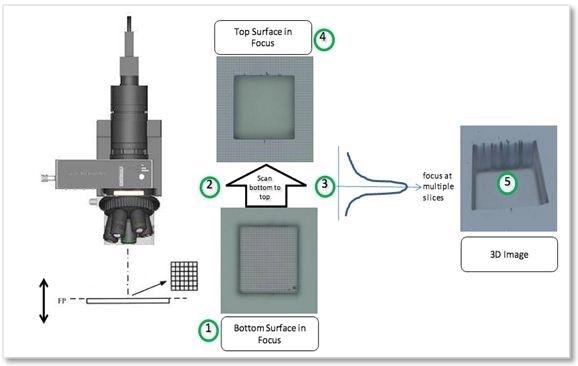
Figure 2. ZDot™ imaging technology
Application Examples
Some of the application examples of the patented ZDot™ imaging technology are as follows:
- Laser power testing
- Semiconductor vias
- Silicon wafer ID
- Microfluidic channels
- Solar cell channels
- LED wafer dicing
- Laser scribing on silicon with thin film
- Coated glass channels
Laser Induced Surface Topography Applications
Laser Power Testing
A leading university is studying the pulsing wattage laser power, and how it relates to the shape and depth of the crater on a wide range of materials. Figure 3 shows the craters that were produced.
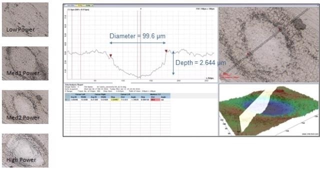
Figure 3. Tungsten substrate with aluminum coating
Vias (Holes) on Flexible Circuits and Wafers
Flexible circuits are extensively utilized in a wide range of industries, such as the automotive, industrial, medical, consumer products, and wearable sectors. These flexible circuits are produced on huge laminated flexible substrates, such as copper foil sheets that are easily deformed and too complicated to manage. This is a daunting prospect for white light interferometers and other conventional optical metrology tools.
The Zeta-20 optical profiler is capable of determining key dimensions, like the depth and diameter of laser drilled blind vias on versatile substrates, at high throughput under production settings. This via has a diameter of 100 µm and a depth of 28 µm. The ZDot™ mode was utilized to produce a true color image. In Figure 4, the color difference on the surface around the blind via can be seen.
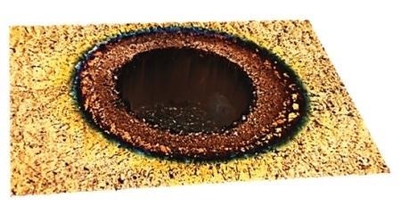
Figure 4. Copper foil
Soft Laser Marking
Due to the wafer warpage induced by conventional hard laser marks, soft laser wafer ID marking methods are being implemented in the semiconductor sector. Wafer real estate is invaluable for fabs operating at the <16 nm node. The idealWafer IDs are shallow and at the same time, they should have sufficient contrast to be read by optical character recognition device.
These features can be automatically determined by locating the low markings on a bare wafer and profiling them with nm resolution at fast throughput. The nanometer ripples induced by the laser can be determined by the Zeta-20 optical profiler, displayed as the red marks in Figure 5.
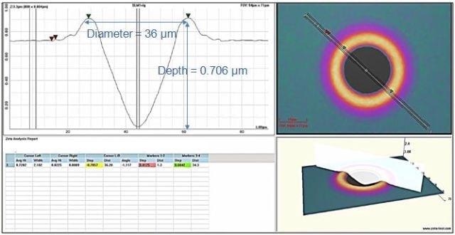
Figure 5. Bare silicon wafer ID mark
The above image was produced by using the ZX100 option.
Laser Scribing of Thin Film Solar
Electrical isolation in thin film solar cells is important, and for this purpose trenches are produced to separate the solar cell’s P and N-doped regions. The laser scribe in certain thin film cells must not breach the underlying substrate made of glass, and should be limited within the area of thin films. In order to boost the absorption of light, the trench can be heavily textured. Solar cells efficiency can be improved considerably by controlling the surface texture and the trench dimensions. This can be realized with ultrafast pulsing lasers to create sharper and cleaner micro-channels. However, it is difficult to automatically locate these trenches on large panels, and provide vital data regarding their width, depth, and roughness.
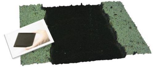
Figure 6. Trench/microchannel on CIGS on glass
The scribe in Figure 6 measures 0.50 and 74µm in depth and width, respectively. The Zeta-20 Optical Profiler employs a high-precision motorized XY stage as well as a pattern recognition software to automatically identify the scribe lines and scan various locations on the solar cell.
Laser Scribing of Micro Fluidic Channel
Microfluidic devices can be used to carry out chemical and biological tests under stringently controlled conditions, by incorporating various fluidic functions in a device. Laser ablation is now substituting lithography methods, and it involves short laser pulses focusing to a small region of the substrate. The crater’s lateral size is controlled by the depth and size of the laser focus by altering the number of pulses. Large side wall slope angles, irregular shapes, heat-induced deformations, low reflectivity, and low image contrast are results of laser processing and present measurement issues for standard confocal profilers and interferometers. The ZDot™ imaging technology combined with the Zeta 3D Feature Detection software provides a number of benefits. The channel depicted in Figure 7 measures 534 and 438 µm in width and depth, respectively.
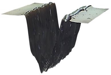
Figure 7. PDMS (polydimethylsiloxane)
Laser Trench Scribing
Indium tin oxide (ITO) is utilized in organics-based electronics and flat panel displays, including organic light emitting devices and transparent electrodes. Laser ablated tranches in ITO provide the potential of highly efficient structuring of transparent conductors on substrates, including glass. As a maskless, dry process, laser direct white (LDW) allows easy modification of the contact pattern. Excellent electrical isolation and well-defined edges at a short isolation between the conductor lines are also needed. When the distance between the conductor lines is reduced to 10 µm, sharp edges are particularly useful. Although a laser confocal tool will be able to reveal interference artifacts on transparent samples with uneven topography, the Zeta-20 Optical Profiler utilizing the ZDot™ mode acquires meaningful data on these transparent samples. The scribe (Figure 8) measures 8.5 and 0.2 µm in width and depth, respectively.
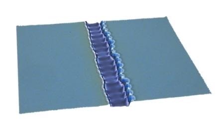
Figure 8. Thin film coated glass (ITO)
LED Die Singulation
Laser scribing is extensively used for isolating an LED wafer into separate dies. This method produces a deep, narrowing trench, leaving behind plenty of debris. This type of geometry prevents the use of laser confocal microscopes, interferometers, and other similar imaging tools. The ZDot™ mode and the highly efficient optical design allow the collection of the maximum amount of light from such samples. The scribe (Figure 9) measures 15.84 and 9.1 µm in depth and diameter, respectively, with rough and tapering side walls.
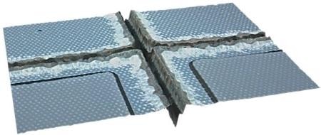
Figure 9. Gallium nitride on sapphire wafer
Laser Scribe
Producing an only minimum amount of debris, laser scribes can precisely mark defects on a wide range of substrates.
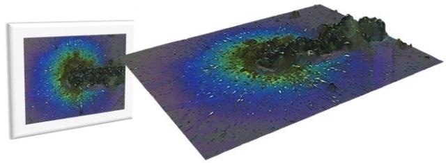
Figure 10. Thin film coated silicon
Figure 10 shows a test laser scribe produced on a thin film coated silicon surface. The True Color Zeta-20 Optical Profiler data is used to calibrate and tune the laser for suitable scribing. Issues like low reflectivity, high sample roughness, and debris present challenges for traditional interferometers. Such surfaces can be dealt with the ZDot™ mode on the Zeta-20 optical profilers.

This information has been sourced, reviewed and adapted from materials provided by KLA Corporation.
For more information on this source, please visit KLA Corporation.