The KLA Nano Indenter G200 laser heater system (Figure1) is considered the most flexible and user-friendly instrument in the world and has been specifically developed for high-temperature mechanical testing at nanoscale. The system uses a laser as a very fast heating method to provide stable and accurate testing conditions for elevated nanoindentation. The main features of the system include its ability to continuously measure the various nanomechanical properties as a function of depth, e.g. modulus and hardness at precisely controlled temperatures up to 500 °C (0.1 °C accuracy).
In order to ensure reliable data, the KLA Nano Indenter G200 laser heater system reduces thermal drift by simultaneously heating the tip using laser heater. In addition, the system is fully integrated with NanoSuite software and can be used with a range of methods including dynamic measurements enabled by Continuous Stiffness Measurement (CSM) option.
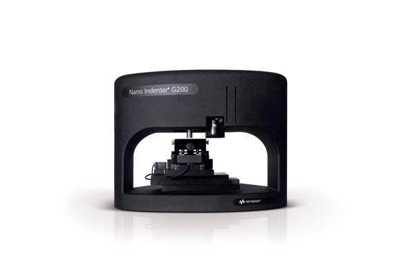
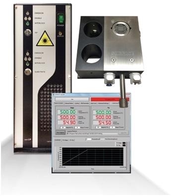
Figure 1. The KLA Nano Indenter G200 (top) and Laser Heater System (bottom, which includes the stage, controller and software interface).
The G200 laser heater system uses laser heating technology to independently heat up the sample and indenter tip with minimum thermal drift (Figure 2). To achieve the tip heating while keeping the benefits of laser heating of the sample, a thin optical fiber is installed inside the hollow shaft of the XP head and heats a special tip with integrate thermocouple. Independent temperature settings for tip and sample enable the optimization of temperature-dependent indentation tests.
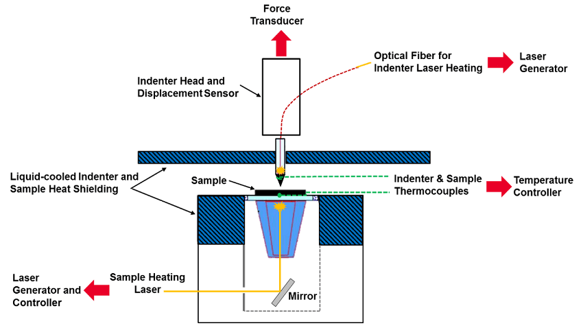
Figure 2. Schematic of KLA G200 laser heater system for high-temperature nanoindentation.
This article will begin with the general problems and challenges that high-temperature indentation measurement is currently facing. Next we will evaluate the mechanical properties test of pure titanium at a broad range of temperatures from ambient temperature to 500 °C, using the laser heater along with CSM method to accurately examine the temperature and depth dependence of Ti at different temperatures. In another demonstration, the creep behavior and plasticity transition of a standard (100) silicon wafer is also studied under increased temperatures up to 500 °C.
Problems and Challenges for Nanoindentation at High Temperature
High-temperature nanoindentation measurements are particularly challenging. High accuracy of displacement measurements with nanometer resolution can be easily influenced by any change in thermal stability during the test, and a very small variation in the temperature can cause a considerable thermal drift. These errors in time-dependent displacement measurements usually arise from nanoindentation system frame drift, or indenter-sample contact drift, or both.
Utilizing large heating elements in conventional high-temperature nanoindentation regularly takes several hours for the temperature to stabilize, as it needs to minimize the thermal gradients existing in all the heated and cooled components in the system.
Another source of thermal drift is contact drift. This depends on factors such as thermal gradient, material properties, contact area, etc. To eliminate thermal drift, it is essential to minimize both types of drifts. However, the waiting time strongly depends on the testing time and temperature. The indenter-sample thermal gradient may never be completely removed during dynamic measurements, where the contact area is changing as the indenter is advancing into the surface of the sample.
To resolve this issue as discussed in the following content, independently and simultaneously heating and monitoring the temperature of both the indenter and the sample has been demonstrated as the best and fastest way for temperature matching between the indenter and sample.
Elevated Nanoindentation on Pure Ti at a Wide Range of Temperatures
Titanium (Ti) and titanium alloys are attractive materials for high temperature applications as they have excellent high temperature stability, creep resistance, good corrosion, and high strength. These properties can be considerably improved by chemically modifying the microstructure of the titanium material, for example, there are some developed grades of titanium alloys that can operate at service temperatures as high as 500 °C. With its high strength-to-density ratio and superior elevated mechanical properties, titanium is a competitive candidate with commonly used stainless steels and nickel-based superalloys in similar applications.
During the elevated nanoindentation test, the sample surface of pure Ti which is commercially available was mechanically polished for nanoindentation test. The test involves mounting the sample in a specially designed laser heater stage that is fitted with a thermocouple and connected to the sample to report the exact temperature during the test in situ. The stage was then moved under the XP indenter (diamond berkovich), designed to be also heated by laser to the required testing temperature. The indenter tip is attached with a fine thermocouple to obtain the most accurate measurements of tip temperature, which corresponds with the sample temperature for contact drift minimization. Laser heater control software is used to control the rate of heating and testing temperatures for both the tip and sample. Standard CSM method was employed for temperatures beginning from 20 °C and going up to 200 °C, 400 °C, 450 °C and 500 °C.
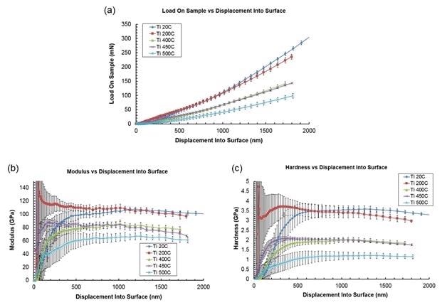
Figure 3. a) Load b) Young’s Modulus and c) Hardness at different indentation depth for pure Ti at room and elevated temperatures using G200 laser heater system and Continuous Stiffness Measurement (CSM) method.
The results are shown in Figure 3, indicating a major decrease in the force load, Young’s modulus, and hardness with increasing temperature as predicted. For each test temperature, all curves are averaged over 9 data series. It is clear that beyond 500nm depth hardness and modulus values become constant.
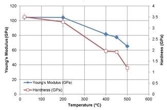
Figure 4. Young’s modulus and hardness of Ti as a function of Temperature.
Shown in Figure 4 are the modulus and hardness data obtained for all test temperatures and averaged over the depth range of 500 to 1700 nm. The values are summarized in Table 1. The data illustrates that Ti’s mechanical properties are maintained at 200 °C as there is no considerable change when compared to the room temperature properties. However, as the temperature increases to 400 °C, the values reduce dramatically because of the softening behavior of Ti at extreme temperatures.
Table 1. Comparison of hardness and modulus of Ti at different temperatures
Temperature
(°C) |
Young's Modulus
(GPa) |
Std. deviation
(GPa) |
Hardness
(GPa) |
Std. deviation
(GPa) |
| 20 |
104.6 |
1.5 |
3.5 |
0.1 |
| 200 |
104.3 |
3.3 |
3.3 |
0.2 |
| 400 |
81.5 |
2.6 |
2.0 |
0.1 |
| 450 |
77.6 |
1.9 |
1.9 |
0.1 |
| 500 |
65.2 |
4.4 |
1.2 |
0.2 |
Brittle-to-Ductile Plasticity Transition Behavior Study of Silicon Using High-Temperature Nanoindentation
The semiconductor industry extensively uses single crystal silicon (SC-Si) to make micro and nano electronic devices. One major practical importance in the development and manufacture of these devices is the brittle-ductile transition (BDT) of single crystal silicon (SC-Si), as these devices require several thermomechanical processing steps. Understanding the material behavior, i.e., phase transformation and deformation mechanisms not only improves control and but also helps predicting Si failure during thermomechanical processing. One key thermomechanical properties of many materials is that they become ductile at higher temperatures and are brittle at low temperatures. This transition takes place over a narrow temperature range for Si, known as brittle-to-ductile transition temperature (TBD).
Fluctuating temperatures during the primary mechanical testing methods, such as fracture toughness test, is one way of measuring the transition plasticity of materials that are difficult to be tested on the nano-scale, which is used to detect the scale-sensitivity of these transitions. At elevated temperatures, nanoindentation allows accurate measurement of Si’s nanomechanical response at numerous temperatures as well as the evaluation of the plasticity transition. This is very important to improve the electronic device fabrication methods.
A large increase in dislocation density in the microstructure and their increased mobility in response to temperature would have contributed to the abrupt increase in fracture toughness. It was observed that for Si, unlike metals, this transition occurs in a very narrow temperature range of 541 to 545 °C for bulk material [1]. It was also demonstrated that this temperature is dependent on size, for example in SC-Si nanowires [2], when there is a reduction in the sample size, TBD reduces to a couple of hundreds degree C (250 °C) from what was seen in bulk material (545 °C) [1]. As illustrated in Figure 5a-c, changes in the plasticity behavior at numerous testing temperatures can also be reflected on the loading-unloading nanoindentation curves. The figure demonstrates that when the temperature is increased from room temperature to 250 °C, no major difference is seen in the maximum indentation depth or behavior of loading-unloading nanoindentation curves. Yet, loading-unloading indentation hysteresis at 500 °C shows larger penetration depth and deformation.
Given the Si phase transformations and their corresponding volumetric changes during loading-unloading at room temperature, a clear displacement discontinuity is seen in the curves (indicated by the arrow) in Figure 5a. This displacement discontinuity is controlled by the amount of deviatoric and hydrostatic stress components under the indenter tip, which is also highly dependent on the tip geometry. Such kinds of defective loading-unloading curves can be due to the formation of deep lateral cracks under the indenter tip. The steps observed on unloading curves are known as pop-outs, perhaps caused by the transition to the lower density structures related to a volumetric expansion. At higher testing temperatures of 250 °C and 500 °C, no evidence of such events are observed and the load-penetration curves appear to be well-behaved (Figure 5b-c).
When the creep behavior of Si (dashed boxes in Figure 5a-c) was examined in more detail, it was observed that at a constant peak load of 570 mN, the material experienced a major deformation over time at 500 °C, as shown in Figure 5d. These curves demonstrate virtually no changes in displacement into the surface during the 60-second peak holding time at 250 °C and room temperature, while about a 200-nm indentation was observed at the constant peak load at 500 °C.
It is obvious that during indentation at 500 °C, there is a large brittle-to-ductile transition in the plasticity behavior of Si. However, this is lower than what was reported in the literature for bulk SC-Si which was about 545 °C [1]. This may be due to the small-volume and size effect characterization of plasticity behavior existing in nanoindentation.
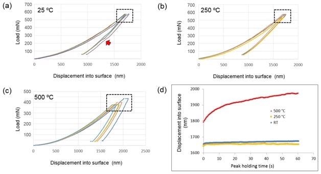
Figure 5. (a-c) Load versus displacement of Si (100) at various temperatures under elevated nanoindentation. (d) The displacement into the surface at peak load (570 mN) versus holding time of the areas highlighted in the dashed boxes.
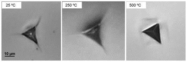
Figure 6. Optical images of indents after nanoindentation at various testing temperatures.
Shown in Figure 6 is the indentation shape after unloading which was obtained by optical imaging at various testing temperatures. Evidently, pop-out, brittle cracks, and uniform indent are seen at room temperature. While cracks still appear during indentation at 250 °C, there were no sign of pop-outs. The indentation shape is similar to that at room temperature, but at 500 °C, there were no evidence of cracks. In addition, a distinct pile-up was seen around the indenter tip edges with uniform indentation shape that was similar to what was observed in ductile metals such as aluminum (Al). During unloading, no pop-outs were observed either. The above data shows the ductile behavior in Si at 500 °C.
Young’s modulus and hardness measurements acquired from the above-mentioned tests are compared in Table 2. Results demonstrate that while there is a decrease in the hardness and modulus of Si at 250 °C, the change is not linear when the temperature is increased to 500 °C. This confirms a rapid change in plasticity transition at 500 °C as the hardness and modulus decrease to approximately 40% of those at room temperature.
Table 2. Modulus and hardness of (100) Si at various temperatures under elevated nanoindentation
Temperature
(°C) |
Young's Modulus
(GPa) |
Std. deviation
(GPa) |
Hardness
(GPa) |
Std. deviation
(GPa) |
| 25 |
274.01 |
15.17 |
24.03 |
1.35 |
| 250 |
217.82 |
13.63 |
19.95 |
1.79 |
| 500 |
164.445 |
8.88 |
9.44 |
0.57 |
Conclusions
As a proof-of concept study, the Nano Indenter G200 laser heater system was used to test high-temperature mechanical properties of pure titanium over a temperature range from ambient to 500 °C. Results accurately report the temperature reliance of Ti mechanical properties and the threshold beyond which these properties drop significantly due to microstructural changes by high-temperature material softening. In another test, the nanomechanical response of a single crystal silicon at high temperatures displayed its ductile fracture like metal when the temperature is increased to 500 °C. The plasticity transition from brittle-to-ductile is expressed on the loading-unloading curves.
In summary, using the KLA G200 laser heater for high-temperature nanoindentation measurements allows precise local measurements across the large surface of testing material to acquire data that is more reliable and statistically significant. With high-temperature nanoindentation measurements, scientists can now gain a better insight into the material transition behaviors and, thus, enhance thermal management at elevated temperatures.
References
[1] PB. Hirsch, and SG. Roberts, The brittle-ductile transition in silicon, Philosophical Magazine A, 1991, volume 64, number 1, pages 55-80.
[2] W. Kang, M. Saif, In situ study of size and temperature dependent brittle-to-ductile transition in single crystal silicon, Advanced Functional Materials, 2013 volume 23, number 6, pages 713-719.

This information has been sourced, reviewed and adapted from materials provided by KLA Corporation.
For more information on this source, please visit KLA Corporation.