Also known as surface potential microscopy, Kelvin probe force microscopy (KPFM) is one method in the range of electrical characterization techniques available in atomic force microscopes.
The contact potential difference (CPD) between the cantilever and a surface is mapped during this process, which provides information about the work function and surface potential.
The work-function is defined in solid-state physics as the energy needed to remove an electron from the Fermi level of a solid to the vacuum and is therefore, a surface property and not related to the bulk.
KPFM is a surface-sensitive technique that only analyzes at or near the surface. It is frequently utilized as a qualitative method to gain contrast in relation to the surface potential.
Quantitative scanning Kelvin probe force microscope measurements of the local work function are usually carried out in vacuum. A model is required to outline the electrostatic interactions between the sample and tip, and the work function of the tip must be determined.
The contact potential difference in ambient conditions is affected by surface contaminations of the sample and tip along with surface water films, which also impedes the determination of the work function of a sample surface from the CPD.
How Does it Work?
Kelvin probe force microscopy on Nanosurf AFMs functions in dynamic force mode where a cantilever with a thin electrically conductive coating is directed close to its resonance frequency.
For the majority of KPFM investigations, soft dynamic mode cantilevers coated with platinum-iridium (PtIr) are appropriate and are a similar price to their non-conductive counterparts. As an alternative, cantilevers coated with conductive Platinum silicide or diamond-like carbon can be used, which are more resistant to wear in comparison to PtIr.
The cantilever has an AC voltage applied to it which has a frequency far away from the resonance frequency to quantify the CPD between the cantilever and the surface. An oscillating electrostatic force is generated between the sample and tip which is quantified by a second internal lock-in amplifier in the controller (Figure 1).
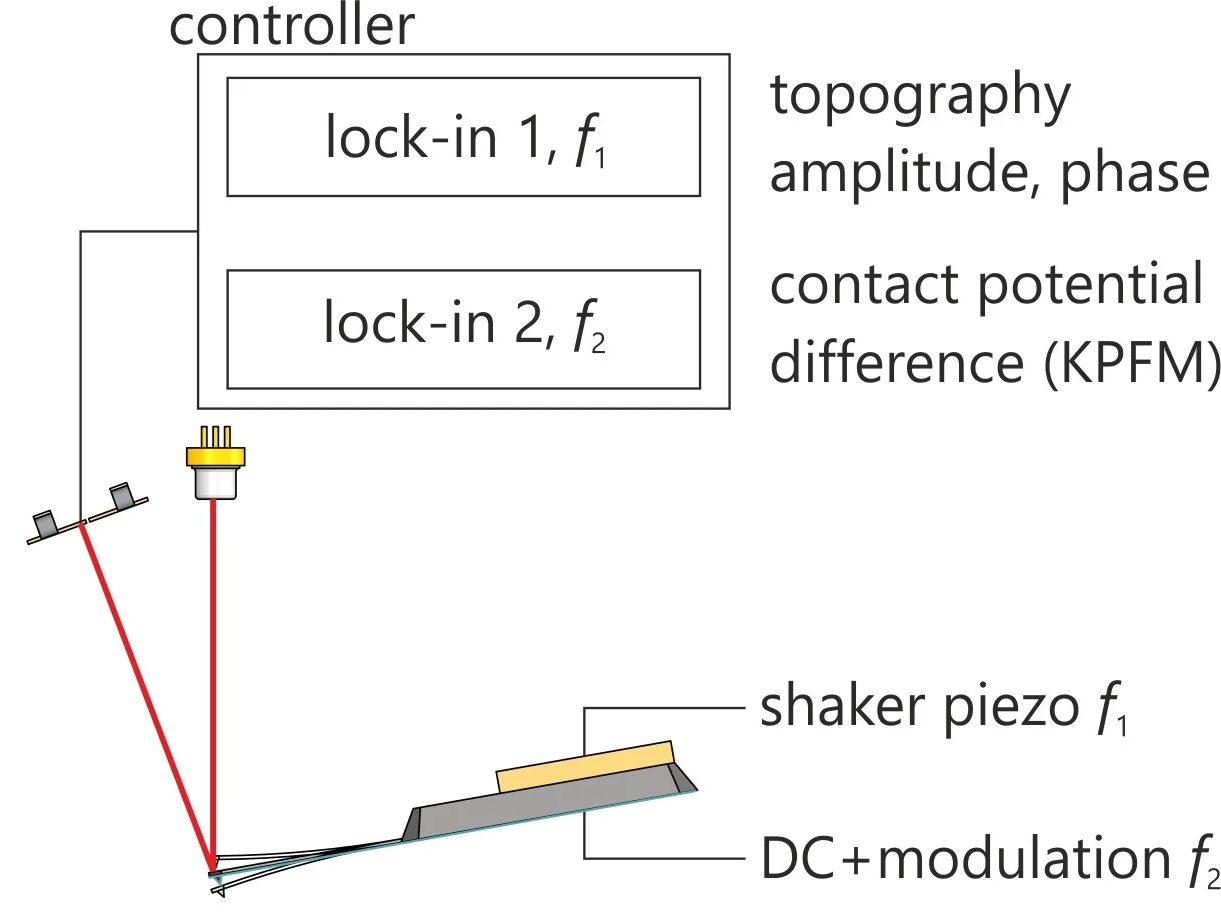
Figure 1. Schematic of KPFM. Image Credit: Nanosurf AG
The cantilever oscillation is canceled out at the AC frequency by adding a DC offset voltage to the AC voltage. A representation of the CPD is produced by recording the applied DC offset voltage as the tip is scanned throughout the surface.
The Nanosurf software features a simple to use KPF routine, which makes configuring KPFM measurements straight forward. This allows even beginner users to gather KPFM data.
KPFM can function in either a dual or single-pass mode. In single-pass mode, the cantilever records CPD and topography while passing over every line once. The benefit of single-pass mode is that correlation between the signals is improved by recording the CPD and topography at the same time.
The KPFM measurement produces higher resolution and sensitivity if the tip is close to the surface, meaning the amplitude of the cantilever oscillation is kept at a low level. Single pass KPFM reduces tip wear and is more efficient, but it is more vulnerable to artifacts at boundaries and edges.
In the dual-pass setup, every line in the image is scanned twice by the cantilever. The topography data is gathered during the first pass. In the second pass, the tip is then lifted or offset above the sample by a distance defined by the user, usually a few tens of nanometers.
As described above, the CPD is recorded. Dual-pass measurements inherently take more time to complete compared to single-pass measurements as every line is scanned twice. It is preferable that the topography captured during the first pass is employed in the second pass to acquire consistent tip-sample separation.
While the time taken to acquire images is longer than the single-pass technique, the advantage is less noisy images and reduced edge and boundary artifacts. The lift height can be decreased by reducing the cantilever’s oscillation during the second pass, which enhances the KPFM contrast.
KPFM Applications
A. Multilayer Graphene: Interesting electrical features can be exhibited by multilayer graphene according to its composition. Figure 2 displays an 8 x 8 µm image at the edge of a graphene flake.
Graphite was mechanically exfoliated and was then transferred to a silicon-silicon dioxide substrate to produce the multilayer graphene flake sample, which was supplied by Hiske Overweg and Klaus Ensslin, ETH Zürich, Switzerland.
The bottom image depicts the KPFM signal overlaid on a 3D surface topography image, while the top image displays the topographical map. In this map, the color contrast shows the contact potential difference or the KPFM signal.
Areas with a green color have low contact potential difference while areas that have a pink or purple color show areas with high contact potential difference.
The electrical characteristics at various thicknesses of the flake is shown in this CPD map as the thin flakes on top have high contact potential (blue) while the rest of the layer has a smaller contact potential (green).
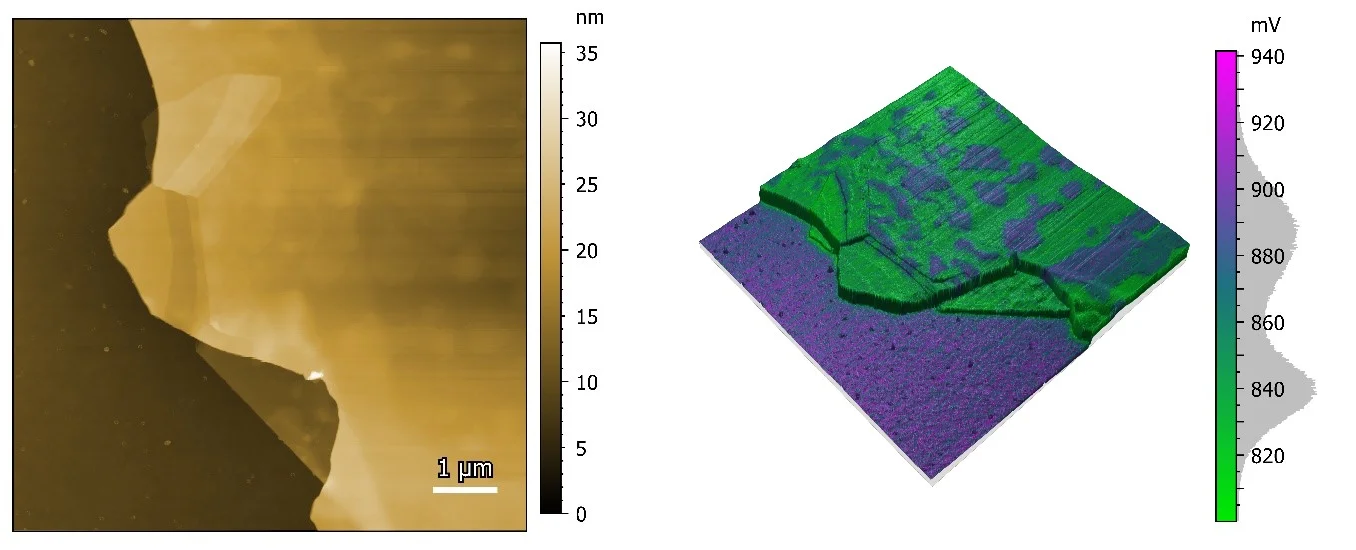
Figure 2. Multilayer graphene. The left image is an 8 x 8 µm2 topography image while the right image shows the 3D representation of the surface topography overlaid with the contact potential difference. Image Credit: Sample courtesy of Hiske Overweg and Klaus Ensslin, ETH Zürich, Switzerland.
B. MoS2 Monolayer: The analysis of a molybdenum disulfide (MoS2) monolayer, which was grown by chemical vapor deposition (CVD), is an example of the efficacy of KPFM, particularly as a technique to reveal electrical properties contrast.
Using a Flex-Axiom, KPFM reveals the contact potential difference variations within a single crystal as well as variations between the single crystal and the underlying SiO2 substrate.
Figure 3 displays an 18 x 18 µm2 image of the monolayer. The bottom image depicts the KPFM signal overlaid on a 3D surface topography image, and the top image is the topographical map.
There is a 650 mV contact potential difference between the substrate and the monolayer even though the monolayer is only 0.6 nm thick. The contact potential signal differs throughout the monolayer, offering information about doping profiles and additional surface defects.
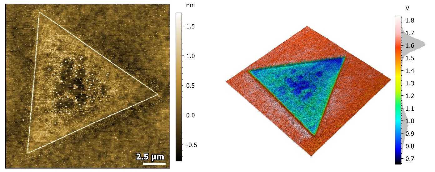
Figure 3. MoS2 Monolayer. The left image is an 18 x 18 µm topography image while the right image shows the 3D representation of the surface topography overlaid with KPFM signal. Image Credit: Nanosurf AG
C. KPFM on Steel: Stainless steel is a metal alloy constructed from composites like aluminum, carbon, and chromium, which are held together in a ferrite matrix. KPFM can be employed to establish how each element is distributed across the alloy as the work potential of each composite within the steel will be slightly different.
Figure 4 shows an 80 x 80 μm image of electrochemically etched and polished stainless steel. The bottom image displays the single-pass KPFM signal while the top image is the topographical map.
The topography image demonstrates that a highly smooth surface (RMS roughness of 3.9 nm) over the 80 μm image was produced by polishing the steel. A difference of 80 mV between the ferrite matrix (green/yellow) and the inclusions (blue) is shown in the KPFM image.
Across the bottom of the KPFM image, the yellow streak was produced by a change to the tip from the defect that can be seen in the bottom left of the topography image.
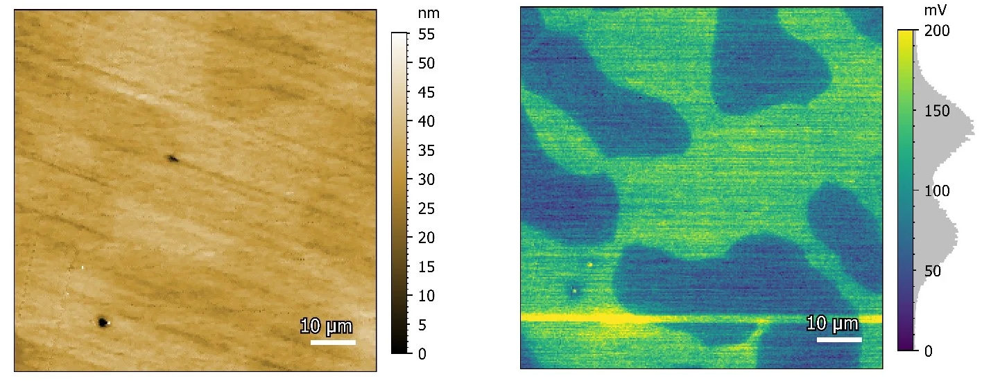
Figure 4. Stainless Steel. The left image is an 80 x 80 μm2 topography image while right image shows the KPFM signal collected simultaneously. Image Credit: Nanosurf AG
D. Insulating Oxide surface: Figure 4 provides an example where dual-pass KPFM was used to image an insulating oxide. Charges were locally deposited in an insulating oxide surface layer in a Swiss-cross pattern in this sample.
The KPFM image on the right clearly displays the location of the buried charges on the surface of the insulating oxide, while the left image is a 10 x 10 µm2 topography image which gives no indication of any Swiss-cross pattern.
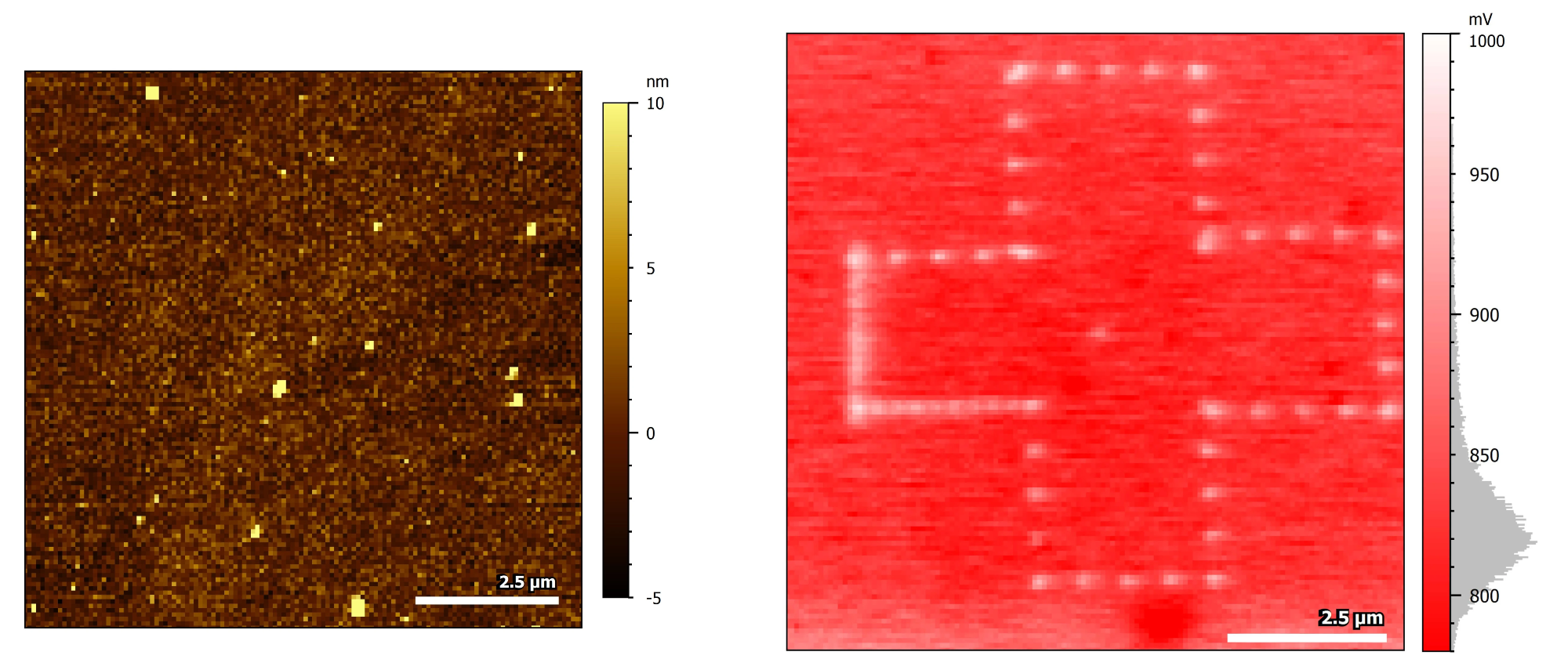
Figure 5. KPFM of locally deposited charges on an insulating oxide surface. The left image shows the surface topography while the right image is the KPFM image. Image Credit: Marcin Kisiel, Thilo Glatzel and students of the Nanocurriculum of the University of Basel, Switzerland.
KPFM as an Improvement Tool for Other Modes
The oscillation of the cantilever is influenced by the contact potential difference between a sample and the tip during dynamic mode imaging. This suggests that the measurement of heterogeneous sample topography in dynamic mode is impacted by differences in contact potential within the sample, which must be compensated.
In other words, the calculated difference in height between two different materials generates an error as a result of the CPD heterogeneity of the materials. This error can be compensated through the use of KPFM feedback during topographical measurements which improves the accuracy of AFM measurements on heterogeneous materials.
This can also be applied to MFM measurements. In MFM, the phase close to the cantilever’s resonance frequency is employed to quantify the force produced by local magnetic dipole moments.
The phase does not differentiate between magnetic and electrostatic forces. The application of KPFM for MFM measurements will decrease the influence of electrostatic forces on the phase shift, which enhances the accuracy of the MFM data.

This information has been sourced, reviewed and adapted from materials provided by Nanosurf AG.
For more information on this source, please visit Nanosurf AG.