In precision imaging of various biochemical phenomena, gold-coated surfaces play a role that is growing with importance.
There are many unique qualities that make gold surfaces perfect for atomic-scale observations, including useful adsorption properties with bioactive implications and near-total (>99%) reflectivity in the infrared (IR) region.
In numerous types of IR spectroscopy, this has proven pivotal, where gold-coated glass is employed as a substrate for biomolecules of interest. Mica and glass are not the only substrates utilized for microscopy-grade gold thin films.
Platypus Technologies engineer gold-coated silicon wafers which exploit the unique electrical conductivity of both the coating and the substrate to allow advanced electrochemical experimentation
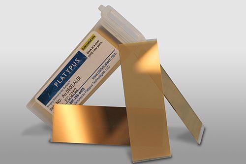
Image Credit: Platypus Technologies, LLC
Outlining Gold-Coated Silicon Wafers
Generally, silicon wafers act as the underlying surface for microelectronic devices like hard drive devices (HDDs) and integrated chips (ICs). This is because of their unique semiconducting properties, which are inherent to silicon and determined by the presence of certain chemical dopants.
Silicon wafers can be engineered for specific charge-carrying capabilities by modulating these electrical properties, and they can be utilized as electrodes for a wide scope of applications, like electrochemical impedance spectroscopy (EIS).
What is Electrochemical Impedance Spectroscopy?
EIS gives detailed insights into complex phenomena such as surface sensitivity and electron transfer resistance and is one of the most sophisticated types of electrochemical research. It is performed by immobilizing an analyte on a semiconducting surface under an applied voltage and measuring the current response.
In order to enable their use in EIS, silicon wafers must sometimes be functionalized using a secondary interface material. Ultra-thin gold coatings are the ideal solution for electrochemistry silicon substrates because of their useful electronic characteristics and exceptional planarity.
Platypus Technologies’ gold-coated silicon wafers have been utilized to assess a large range of key reaction mechanisms and electrochemical phenomena using EIS. The performance of desalination membranes as a function of salt permeability of polyamide films is among these.
It was possible to establish the differential resistance of the polyamide films by the thickness and solution concentration with angstrom-scale topographical uniformity and outstanding surface purity, giving better insights into osmotic membrane desalination performance.
Gold-Coated Silicon Wafers from Platypus Technologies
Platypus Technologies has developed a cutting-edge workflow for developing custom gold-coated silicon wafers for microscopy and electrochemistry.
All of their substrates are based on electron beam physical vapor deposition of high-purity gold targets, with high degrees of adhesion between underlying substrates and gold thin films promoted by an intermediary titanium adhesion layer.

This information has been sourced, reviewed and adapted from materials provided by Platypus Technologies, LLC.
For more information on this source, please visit Platypus Technologies, LLC.