Due to the nature of light, a traditional optical microscope can be employed to attain a maximum magnification of around 800–1000x. For further magnification, scanning electron microscopes (SEMs) can be used, in this case the transmission electron microscopes (TEMs) can identify single atoms and so provide the highest magnification possible.
Considering this information, why is the scanning probe microscope (SPM) employed as yet another type of microscope? One reason is that a to-be-investigated sample in a transmission electron microscope has to be thinly sliced and so could be damaged.
The SPM technique involves imaging surface structures without ruining the sample at atomic (height) resolution. The type of imaging provided by SPM microscopes is another reason since the outcomes are shown as a type of 3D image (also in instances where only 2D information is examined).
It is difficult to analyze the surface structure of a sample by utilizing an electron microscope since this is the scenario with an optical microscope. The sample has to be sliced to measure a surface profile with the highest resolution.
An SPM also works in the absence of vacuum and contrary to optical and electron microscopes, it can measure other physical influences. This includes magnetic characteristics (Magnetic Force Microscopy, MFM) and electrical characteristics, such as Kelvin Probe Force Microscopy (KPM/KPFM).
Image Credit: Semilab Semiconductor Physics Laboratory
Types of Scanning Probe Microscopes
DC Mode
The purported DC, or contact mode is the most fundamental AFM operation mode. In this technique, a force is applied to the cantilever (sensing) tip when the sample surface and the cantilever are near to each other. This leads to the bending of the cantilever, which alters the detection laser’s reflectance angle.
In order to measure the deflection of the laser a position-sensitive photodetector is utilized. Upon moving the cantilever toward the sample during the process attractive forces are applied to the cantilever. By utilizing these negative forces a surface scan can be performed.
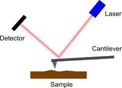
DC Mode. Image Credit: Semilab Semiconductor Physics Laboratory
AC Mode
Currently most AFM microscopes are operated in the purported AC mode instead of the DC mode to prevent damage to the cantilever. In this mode an extremely low force is employed during the scanning process, and minimal interaction occurs between the cantilever and the surface without resolution loss.
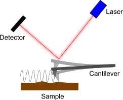
AC Mode. Image Credit: Semilab Semiconductor Physics Laboratory
The cantilever is made to vibrate with its resonance frequency permanently. This oscillation leads to a periodic bending of the cantilever, which can be calculated by utilizing a reflected laser beam like in DC mode.
When the cantilever is close to the surface and interacts with the surface atoms there is an alteration in the resonance frequency. (In fact, there is an increase in the resonance frequency when the cantilever reaches the surface.)
This leads to a dampening of the amplitude and a modification in the phase of the cantilever oscillation. The dampening of the cantilever oscillation and the tip-sample interaction force are roughly proportional when the tip is close to the sample.
The AC mode works with less interaction force when compared to the DC mode, and it has certain advantages:
- It is possible to utilize a single cantilever for more images due to the lower forces
- It is possible to image fragile samples in AC mode, which otherwise would be damaged in a DC measurement
- The relation phase shift/damping is attributive to the surface material, so more information can be obtained using this operation mode
- Due to the low interaction forces the surface itself is considerably less affected by the measurement
Magnetic Force Microscopy - MFM
In order to detect magnetic forces a cantilever must be utilized, this is applied with a magnetic coating. Standard MFM tips include a magnetic coating which has a comparatively large thickness of about 40 nm. The high thickness results in a much larger tip radius of about 50 nm, which is considerably larger compared to that of traditional AFM tips.
These standard tips can be employed to attain lateral magnetic resolutions of approximately 100 nm. So, compared to the commonly expected resolution from AFM topography measurements, which are better by a factor of 10, the magnetic resolution is much less.
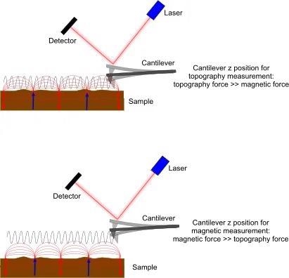
MFM. Image Credit: Semilab Semiconductor Physics Laboratory
Mechanical force and magnetic force also contribute to the force measured by the cantilever when the MFM tip is near to the sample. Although the magnetic force is is effective over long distances, it is considerably smaller compared to the mechanical force.
The two sources of force can be separated by measuring the MFM force from a specific distance of the sample surface, where the contribution from the mechanical force can be ignored.
Kelvin Probe Force Microscopy - KPFM
This mode can be used as a method for establishing the chemical potential between a cantilever and a sample surface to gather information related to the material and the material state on a sample surface. The basic framework for performing a KPFM measurement is shown in the figure below.
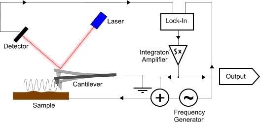
KPFM. Image Credit: Semilab Semiconductor Physics Laboratory
An oscillating electric field is produced between the sample and the cantilever when the sample is electrically connected to the output of a frequency generator, and this can be measured by the AFM’s position sensor. This detected signal is then fed into a lock-in amplifier and its output is fed into an integrator.
The outcome is added to the oscillation as a constant offset, which is then applied to the sample. This acts as a feedback loop to reduce the electrically induced cantilever oscillation.
Features
Almost all SPMs can resolve atomic height steps:
- STM provides the benefit that the tunnel current always flows directly over the next atom on the sample surface. This type of “self-focusing” cannot be obtained by utilizing an AFM.
- Normal AFMs are designed for comparatively large scan areas (50–200 µm), and the scanner stages enable the analyses of various sizes and types of samples.
- STMs are typically employed in ultra-high vacuum to ensure that a prepared sample surface stays unaffected for a longer period of time.
- AFMs with lateral atomic resolution are only employed for distinctive applications which necessitate accomplishing a lateral atomic resolution than the loss of flexibility, permitted by the higher stability of the total framework.
- AFMs can achieve lateral atomic resolution.
- STMs are usually incorporated into a highly stable scan platform, and the maximum scan area is around 0.5–10 µm.

This information has been sourced, reviewed and adapted from materials provided by Semilab Semiconductor Physics Laboratory.
For more information on this source, please visit Semilab Semiconductor Physics Laboratory.