It is possible to generate long-range wavelength ordering known as Moiré superlattice periodicity by stacking two-dimensional (2D) materials within each other’s van der Waals interaction distance.
When this process is applied to graphene on hexagonal boron nitride (hBN), this effect would appear on the uppermost layer of graphene, causing graphene’s energy bandgap to open.1,2,3
Regulating lattice orientation between graphene and boron nitride can facilitate variation in the Moiré periodicity's wavelength, effectively tuning the graphene energy bandgap. The energy bandgap range will, in turn, affect graphene’s performance and device functionalities.4
Researchers will therefore benefit from a simple means of deciphering Moiré shape and periodicity, particularly when designing 2D graphene/BN-like heterostructured devices and materials.
Piezo-response Force Microscopy (PFM) is a technique utilizing contact Atomic Force Microscopy (AFM)-based imaging, commonly employed when there is a need to electromechanically map a sample with nanoscale lateral resolution.
PFM has demonstrated good potential for the detection of local strain gradients and piezoelectricity in a range of 2D heterostructured material systems, such as graphene/hBN.5
This article explores the use of contact resonance PFM in characterizing Moiré shape and periodicity of the superlattice wavelength. The experiments presented here utilize two types of graphene-on-hBN stacked systems, and these variables are correlated in order to illustrate lattice misalignment and rotation.
Experiment and Result
Monolayer Graphene on Hexagonal Boron Nitride
The sample presented in this example was a monolayer graphene that had been epitaxially grown on a hexagonal boron nitride. The PFM setup was comprised of a Park NX10 AFM system used in conjunction with a Zurich Instruments HF2 lock-in amplifier.6
The PFM cantilever probe (PPP-EFM) in use was a ~3 N/m Si cantilever probe. The probe had been PtIr-coated and had an air resonance of ~75 kHz. The AC voltage used in this example was 2 V, while a ~330 kHz contact resonance frequency was also utilized.
AFM loading force applied during PFM scanning was 40 nN, while the PFM scan rate was set at 1-1.5 Hz. Scan size data of 100 nm x 100 nm and 200 nm x 200 nm was obtained.
Contact resonance PFM was performed on the graphene sample according to the procedure defined by Hermes et al., who successfully used PFM to image ferroelectric domains in Bismuth Ferrite (BFO).6
There was a single exception in the PFM study on BFO, however. Surface pits inhibited the contact resonance frequency, preventing this from remaining within acceptable levels during the scanning process.
This meant that it was necessary to enable ‘Double Frequency Resonance Tracking’ (DFRT)’s PID control throughout the scanning process, therefore compensating for shifts occurring within contact resonant frequency.
The topography of graphene/hBN in the scanning area featured here is atomically flat and almost featureless. Because of this, the contact resonance frequency shift during the PFM operation is negligible, therefore facilitating high-resolution PFM data with no need to use DFRT's PID control.
Figure 1a displays a contact-resonance PFM amplitude image with a honeycomb Moiré periodicity. The periodic superlattice spacing in this example is 15 nm, which is two orders of magnitude larger than graphene and hBN’s atomic lattice constants.
A Moiré periodicity of ~14-15 nm is expected for aligned graphene on boron nitride 2,3, and the results from this experiment were found to be consistent with this value.
The sample also showed a consistent 15 nm periodicity and a coherent piezo-response signal when zoomed out to 200 nm x 200 nm and scanned again (Figure 1b).
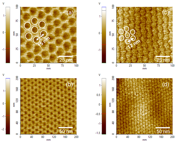
Figure 1. PFM amplitude images. Honeycomb Moiré patterns with periodicity 15 nm on monolayer graphene/hBN (a) and (b), and with periodicity 12 nm on twisted bilayer graphene/hBN (c) and (d). Image Credit: Park Systems
Twisted Bilayer Graphene on Hexagonal Boron Nitride
An exfoliation technique was used to prepare the sample in this experiment, with the upper graphene bilayer graphene deliberately misaligned by 1.15 degrees in relation to the underlying hBN substrate.
The exfoliated bilayer graphene’s surface was investigated using non-contact AFM survey imaging. This revealed a residue film with a nanometer-scale thickness covering the exfoliated sample surface - likely left over from the exfoliation process itself.
A PPP-EFM probe was initially used to scan the sample in contact mode AFM. This was done using up to ~500 nN loading force, allowing the probe to effectively sweep aside the residue. A new PPP-EFM probe was then used to undertake PFM measurements on the newly cleaned bilayer graphene surface.
PFM setup and imaging procedures employed in characterizing the deliberately misaligned bilayer graphene were identical to those used to characterize the monolayer graphene, with the exception of the following parameters:
- AC voltage applied was 6 V
- Contact resonance frequency was 354 kHz
- AFM loading force applied during PFM scanning was 500 nN
- PFM scan rate was 2-3 Hz.
A 100 nm x 100 nm scan contact-resonance PFM amplitude image can be seen in Figure 1c. This image shows a hexagonal pattern which allowed the team conducting this experiment to determine that the misaligned bilayer's superlattice periodicity was 12 nm.
A 20% difference in Moiré periodicity was detected between bilayer graphene and monolayer graphene, with the latter being the larger of the two. Ideally, the 12 nm wavelength periodicity will correspond to the bilayer graphene's configuration misaligned by the 1.15-degree twist on BN.
Monolayer graphene with 15 nm periodicity, therefore, represented monolayer graphene on hBN with no misorientation between the two layers.
This observation is in line with the general principle that the Moiré periodicity (superlattice wavelength) is further reduced as misalignment becomes more prevalent between the top adlayer and the underlying layer.7
Figure 1d displays PFM amplitude data of the same area, zoomed out to the 200 nm x 200 nm scan area.
Individual components making up the honeycomb array can be observed with the same periodicity in both the zoomed-in and zoomed-out scan images of Figures 1c and 1d.
Summary
The experiments outlined here saw Moiré superlattice periodicity in two types of graphene on hexagonal boron nitride structures successfully characterized using contact resonance PFM.
Bilayer graphene was misoriented with a 1.15-degree twist on hBN. This resulted in a 12 nm Moiré wavelength periodicity - 20% smaller than the 15 nm lattice periodicity observed on monolayer graphene on hBN.
Formation of a Moiré superlattice possessing a wavelength of 14-15 nm is known to be highly characteristic of aligned monolayer graphene on hBN.
This, therefore, confirms that contact resonance PFM is an appropriate quality control technique due to its ability to accurately ascertain Moiré periodicity in graphene/hBN-like 2D multi-layered samples.
References
- S. Tang et al., Scientific Reports 3(2666) 2013.
- C. Woods et al., Nature Physics 10 (2014) 451–6.
- A. Zandiatashbar, B. Kim, Y. Yoo and K. Lee, Microscopy Today, Volume 23, Issue 6, November 2015, pp. 26 – 31.
- Z. Zheng, Q. Ma et al., Nature, 588 (2020) 71-76
- L.J. McGilly et al., arXiv:1912.06629 [cond-mat.mes-hall]
- I. Hermes and R. Stomp, Park AFM Application Note: DFRT PFM. https://parksystems.com/images/media/appnote/DFRT-PFM_AppNote_Park-Systems.pdf
- N. Neek-Amal and F. M. Peeters, Appl. Phys. Lett., 104 (2014) 041909
Acknowledgements
Produced from materials originally authored by Byong Kim, John Paul Pineda, Ben Schoenek, Jiali Zhang, Armando Melgarejo (Research Technical Services, Park Systems, Inc.), Qiong Ma (Department of Physics, Boston College), Ilka Hermes (Applications, Park Systems Europe GmbH.) and Dae Yoen Won (Research & Development, Park Systems Corp.).

This information has been sourced, reviewed and adapted from materials provided by Park Systems.
For more information on this source, please visit Park Systems.