The Park FX300 is a real game-changer in atomic force microscopy since it is made to blur the lines between research and industry applications. It supports several AFM techniques tailored for reliability assurance, quality control, and research. Industry-specific research options, including accurate wafer-level alignment and orientation control and surface roughness assessment over wide areas, are offered by the Park FX300.
It has improved optical setups for better sample vision and contamination control in extremely clean measurement settings. Because of these characteristics, the Park FX300 is an essential tool for wafer-level packing, semiconductor post-processing, and other cutting-edge industrial R&D applications.
Advanced Capabilities for Industrial & Research AFM Applications
300 mm Wafer Measurement Supporting Advanced Applications
It supports various sophisticated AFM applications, including the optional AFM-IR technology, and can measure wafers up to 300 mm.
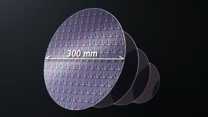
Image Credit: Park Systems
Specialized Industrial R&D Applications
Specialized industrial R&D applications with a rotatable stage, routine measurements based on recipes, and long-range surface roughness profiling.
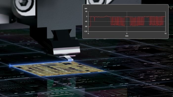
Image Credit: Park Systems
Enhanced Optical Sample Visualization
Advanced off-axis optical configurations are optional and can improve sample visualization.
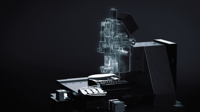
Image Credit: Park Systems
Integrated Industrial-Grade Facility
An integrated industrial-grade facility with a signal tower, an emergency-off unit, a facility controller, and an optional fan filter unit for contamination management.
Image Credit: Park Systems
Intelligent Automation
It increases efficiency by automating crucial processes like laser alignment, parameter adjustment, and probe recognition and exchange. To decrease downtime and increase efficiency, it has 16 probe slots for repeated measurements and mode transitions.
Automatic Probe Type Recognition
A new probe's chip carrier has a QR code that the Probe Identification Camera reads to display all relevant information about each tip, such as kind, model, application, and usage. This allows the user to quickly choose the ideal probe tip for each task, guaranteeing precision and effectiveness.
Automatic Probe Exchange
Thanks to automated probe exchange, old probes can be readily and securely replaced with complete automation. With 16 probe slots for frequent measurements and mode changes, it minimizes downtime and boosts productivity with quick, self-switching probe swapping.
Automatic Laser Beam Alignment
Automatic Beam Alignment maximizes the spot’s position on the PSPD in vertical and lateral directions by aligning the laser beam with the appropriate cantilever. At the touch of a button, it automatically moves the X, Y, and Z axes to produce sharper, distortion-free images.
Simplified Operation
Automatic Sequential Measurement
It enables automated execution of predetermined coordinate settings on big samples, including 300 mm wafers or samples on a multi-sample chuck. It streamlines processes in industrial and research settings by sequentially supporting enhanced modes and topographical measurements.
Next-Generation AFM Controller for High-End Products
The Park FX Controller was created primarily to improve the Park FX Series’ performance. Advanced Piezoresponse Force Microscopy (PFM) applications, like Contact Resonance PFM (CR-PFM) and Dual-Frequency Resonance Tracking (DFRT-PFM), are made possible by this important advancement without requiring extra hardware. This guarantees that the clients may benefit fully from the most recent developments in atomic force microscopy.
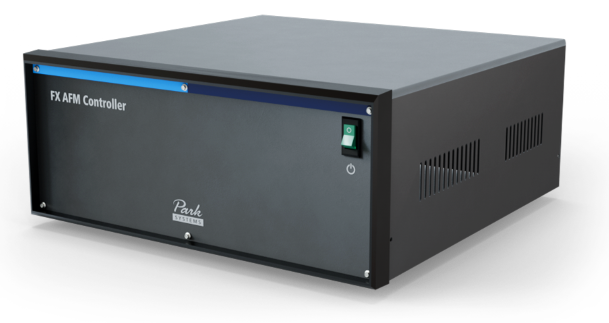
Image Credit: Park Systems
- DFRT-PFM without the need for external amplifiers
- Direct CR-PFM enablement with greater bandwidth for tip bias modulation
- Improved Safety and Real-Time Monitoring of the Environment
- Faster Ethernet connectivity for efficient data and image processing
Park AFM-IR Spectroscopy
Advanced AFM-IR Spectroscopy for Large Sample Chemical Analysis
The Park AFM-IR system combines atomic force microscopy (AFM) and infrared (IR) spectroscopy. Chemical identification is provided via the spectroscopic portion with a spatial precision of 5 nm.
It employs a non-contact method with the highest industry spatial resolution and the safest spectroscopy scanning. The microscopy portion gives users information on mechanical properties and nanometer 3D topography with sub-angstrom height accuracy.
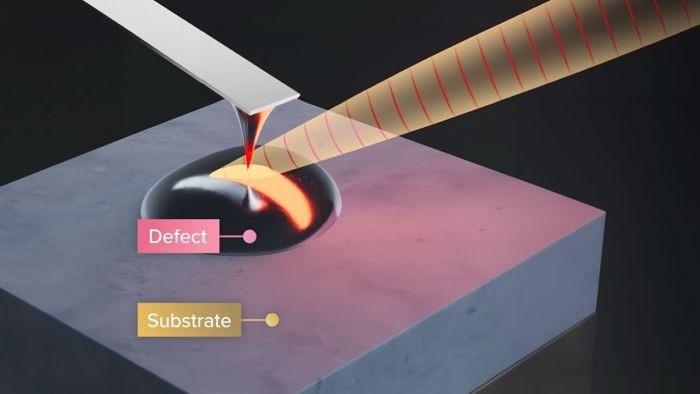
Image Credit: Park Systems