Sponsored by Nanosurf AGReviewed by Olivia FrostJan 18 2023
The need to miniaturize electronics has boosted the demand for nano-electrical characterization techniques over the last few decades. Understanding the local electronic material properties such as conductance, dielectric constant, local capacitance, and dopant density is crucial for semiconductor and microelectronics research and development.
Atomic force microscopy (AFM) is a key technique used to link topographical patterns with local electronic characteristics at the nanoscale.
Local currents and electric surface potentials can be measured by using techniques like conductive atomic force microscopy (CAFM) and Kelvin probe force microscopy (KPFM), while scanning capacitance microscopy (SCM) maps the capacitance or local carrier density.
Scanning microwave microscopy (SMM) is unique in its ability to detect buried patterns found in multilayered integrated circuits (ICs). These measurements are critical for applications such as failure analysis, device performance modeling, and process optimization in semiconductor production.
Scanning Microwave Microscopy (SMM)
SMM is a scanning probe technique that analyzes the microwave interactions between a sharp tip and the sample. The microwave reflection coefficient expresses the ratio of power provided to the tip and the power received after being reflected at the tip-sample contact (S11 parameter).
The tip-sample microwave impedance is calculated using the S11 parameter. The microwave impedance provides information on local capacitance, which can be used to calculate the dielectric constant and dopant density.
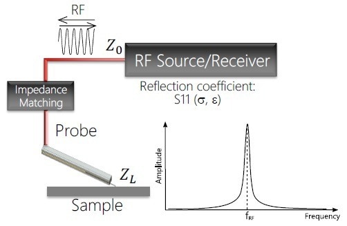
Figure 1. A schematic of a typical SMM setup: RF source/receiver electronics send the RF wave with impedance Z0 through the transmission line to the probe (red). The sample-probe impedance is ZL. The impedance matching circuit works as an “antireflection” medium between the low impedance Z0 and high impedance ZL. There is only one frequency peak (fRF) in the spectrum and the amplitude and/or phase are tracked during scanning of the surface. Image Credit: Nanosurf AG
One of the primary drawbacks of SCM, a technique comparable to SMM, is that dopant density measurements are mostly qualitative and can not be used on materials other than semiconductors.
SMM, on the other hand, can be used to assess a variety of materials, including dielectrics and metals,1 since it does not depend entirely on modification of the depletion capacitance in the sample.
SMM works at higher frequencies, resulting in improved sensitivity, and the high-precision electronics enable calibrated and absolute readings. While extraction of numerical data is possible analytically in SMM, in practice, calibration samples keep the experiment from quickly becoming complex.
A typical SMM configuration includes a radio frequency (RF) wave generator and a receiver operating at a few GHz (Figure 1). In a pure S11 measurement, the transmitter and receiver operate on the same frequency, and the frequency spectrum has just one primary tone (or frequency).
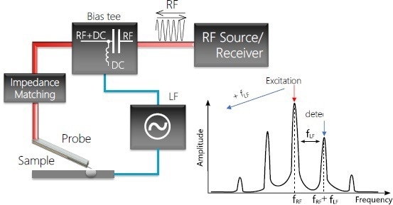
Figure 2. Schematic of a dS11/dV measurement: a low frequency bias voltage (LF) is applied between the probe and the sample. The non-linear behavior of the tip-sample contact causes frequency mixing between the RF and the LF signals. The frequency spectrum exhibits sideband peaks on both sides of the main RF tone (plot). The frequency of the mixed product, i.e. fRF+fLF, is used for detection of dS11/dV. Image Credit: Nanosurf AG
A low-loss coaxial cable transports the signal to and from the cantilever. A matching circuit is often necessary since the normal port impedance is 50 and the tip-sample contact impedance is substantially greater.
The RF electromagnetic wave begins to radiate into free space as it leaves the coaxial line. This can result in topographic cross-talk in the S11 measurement. An AC voltage bias in semiconductor materials can change the dopant density in the sample beneath the tip and, therefore, the S11 signal.
Topographic cross-talk is minimized by tracking the change in S11 relative to the change in bias voltage (similar to lock-in amplification).
This is known as the dS11/dV measurement, and it produces a result similar to the traditional dC/dV measurement in SCM. dS11/dV is solely applicable to semiconductors. A low frequency (LF) is used between the tip and the sample to achieve this measurement. The nonlinearity in the tip-sample interaction results in frequency mixing between the RF and LF waves.
As a result, it produces sideband peaks on both sides of the main tone (Figure 2). The sideband signal is detected by either mixing the signal back down to the LF frequency and demodulating it using a lock-in or directly detecting the amplitude and phase of the sidebands. The latter is preferred as it removes 1/f noise.
SMM Measurements
SMM is used to measure dopant density and analyze failures in semiconductor devices.
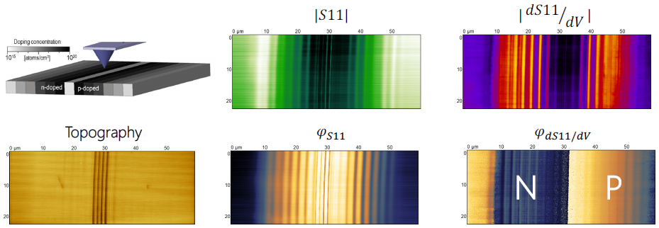
Figure 3. An S11 measurement (amplitude and phase) and a dS11/dV measurement (amplitude and phase) of an Infineon SCM calibration sample. Clear contrast between the regions of different dopant density can be observed in both the S11 and the dS11/dV measurements. The dS11/dV measurement indicates polarity and the type of the dopant – n or p – can be determined. The schematic image of the sample is taken from Ref. 2. Image Credit: Nanosurf AG
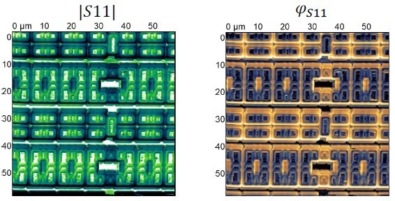
Figure 4. An S11 measurement (amplitude and phase) of a SCM sample, demonstrating high contrast between the areas of different doping levels. Image Credit: Nanosurf AG
Figure 3 illustrates the S11 analysis of the Infineon SCM calibration sample, with high contrast on dopant densities in the 1015-1020 1/cm3 range. The dS11/dV measurement offers additional information, and the kind of dopant (n or p) can be seen in the phase image.
The raw data from the SMM analysis is uncalibrated; hence the calibration technique must be performed on the measured data to derive quantitative values for the capacitance, resistance, and material characteristics. Details of SMM calibration procedures can be found in the literature.2,3
A semiconductor SRAM chip is another example of a structure with distinct changes in dopant type and concentration. Figure 4 depicts an SMM measurement of a device to identify system flaws or relative changes in dopant concentration to assess device performance or potential failure sites.
Conclusion
SMM is a potential substitute for SCM that measures the S11 parameter or the microwave reflection coefficient without the need for resonant circuits. SMM is suitable for materials beyond semiconductors, such as dielectrics and metals.
Calibration is not necessary for many key applications, such as defect detection in the semiconductor industry. Still, analytical calculations are made feasible and material characteristics may be quantified when employing very simple calibration processes.
References
- J. Hoffmann et al., Appl. Phys. Lett. 105 (2014) 013102
- Brinciotti et al., Nanoscale 7 (2015) 14715
- Hoffmann J., et al., IEEE-NANO (2012)

This information has been sourced, reviewed and adapted from materials provided by Nanosurf AG.
For more information on this source, please visit Nanosurf AG.