Graphene is a monolayer of graphite that is of significant interest because of its wide variety of applications in the semiconductor, healthcare, and aerospace fields.
The unique properties of graphene are resulting in novel areas of research, investigating other atomically thin materials which are jointly referred to as “2D materials”.1-6
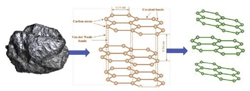
Figure 1. Image of graphite (left); graphite structure (center), and graphene structure (right). Image Credit: H. Sachdeva, “Recent advances in the catalytic applications of GO/rGO for green organic synthesis”, Green Processing and Synthesis 2020, v.9, pp515-537.
One fundamental weakness of graphene transitioning to industrial applications from academic research is the complexity of characterization. As graphene is extremely thin, with one monolayer only being 3.35Å, it necessitates scanning transmission electron microscopy (STEM), atomic force microscopy (AFM), or Raman spectroscopy to characterize it correctly. Although these methods can be highly effective, they each have their limitations.
STEM and AFM are not capable of characterizing the vast areas that would be needed for high-volume production. At the same time, sample moisture absorption can worsen errors in AFM thickness measurement.
Despite Raman spectroscopy being significantly quicker than either STEM or AFM, the measurement time of the method is substantially longer than is viable for high-volume manufacturing. The method for determining the thickness of graphene using Raman spectroscopy comprises a comparison between the spectral peak intensity ratios, which can be challenging due to the extremely small change in ratios after five graphene layers.
This can also be impacted by several other factors, such as the graphene sample’s quality. Finally, all three of these methods can be excessively expensive.
Spectral Reflectance of Graphene
Spectral reflectance is a low-cost method that shows great promise and can be employed to analyze large areas. This method accurately characterizes multi-layer and monolayer graphene stacks on a microscopic scale.8
Graphene is typically characterized by its optical contrast with the underlying substrate. However, this process demands that the optical constants of the system are known while the underlying substrate is of a suitable thickness to achieve sufficient contrast.
Measurement Setup
In this case, spectral reflectance was employed to assess the optical contrast and the spectral shift caused by placing the 2D material on the substrate.
The optical constants of graphene were measured by placing the graphene onto a transparent (fused silica) substrate and utilizing the Filmetrics F10-RT-UVX system to take the measurements. Figure 2 presents the collected reflection and transmission spectra, which were subsequently utilized to establish the optical constants of the material, which are presented in Figure 3. This data allows for thickness characterization across arbitrary substrates.
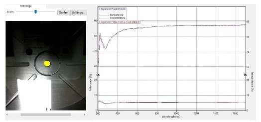
Figure 2. Transmission (upper trace) and reflection (lower trace) data for tri-layer graphene on a fused silica substrate. The layer thickness measured 1.2 nm. Image Credit: KLA Instruments™
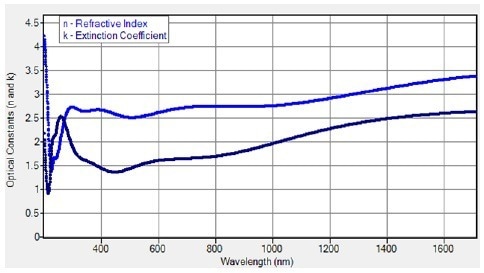
Figure 3. The refractive index (n) and extinction coefficient (k) of graphene were modeled using the reflection and transmission data from graphene on fused silica. Image Credit: KLA Instruments™
The optical constants were then used in the measurement of bilayer and monolayer graphene. As shown in the spectral comparison displayed in Figure 4, there is a significant peak intensity and wavelength shift based on the number of graphene layers.
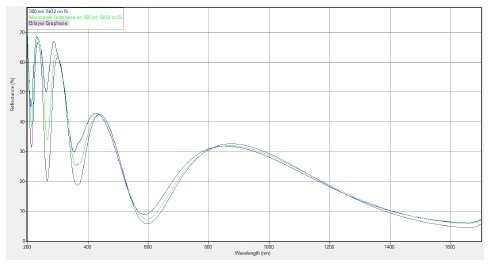
Figure 4. Spectral reflectance spectral comparison of a 300 nm SiO2 wafer (blue), a monolayer of graphene on 300 nm SiO2 (green), and bilayer graphene on 300 nm SiO2 (purple). Image Credit: KLA Instruments™
A significant enough shift can be seen for 300 nm of SiO2 that graphene can be directly observed on these wafers.
The benefit of using spectral reflectance is that it can be used as a characterization method on any arbitrary substrate. It can also be utilized to rapidly characterize graphene over large areas, as demonstrated by the wafer maps displayed in Figure 5, which were produced using the Filmetrics F50 thin film thickness mapping tool.
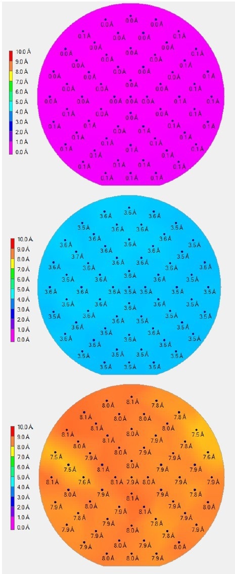
Figure 5. Wafer maps of graphene thickness of 100 mm Si wafers with only 300 nm SiO2, (top), a monolayer of graphene (center), and a bilayer of graphene (bottom), As can be seen, there is a distinct difference in thickness measurement between each wafer, with largely uniform thickness values across each wafer. Image Credit: KLA Instruments™
Conclusions
The Filmetrics F10-RT measurement method can be employed for the extensive area characterization and the determination of optical constants of 2D materials. Future work will seek to study more 2D materials and different orientations of multilayer stacks of graphene.
About the Filmetrics F10-RT-UVX
The Filmetrics F10-RT-UVX Thin-Film Analyzer needs just one mouse click to simultaneously capture transmittance and reflectance spectra by eliminating required hardware configuration changes between measurements.
The true normal incidence design of the F10 is vital for accurately characterizing display films, while the video camera with image capture means that measurement location is simple and recordable.
The industry-standard FILMeasure software provides the power of Filmetrics analysis to deliver accurate measurements for various application types.
About the Filmetrics F50-UVX
The Filmetrics F50 is a thin film mapping tool that can measure samples up to 450 mm in diameter. The automatic movement of the motorized R-theta stage to the measurement point delivers thickness measurements as rapidly as two points per second.
The F50 is equipped with predefined map patterns and the option for users to create their own patterns. This enables users to set up and run measurements in minutes.
Contact KLA Instruments to schedule thickness measurement on your film samples, or to conduct 3D surface topography with the Filmetrics Profilm3D® optical profiler, which easily and rapidly produces surface measurements of step height, roughness, or other features of interest.
References and Further Reading
- S.J. Kim, K Choi, B. Lee, Y. Kim, and B.H. Hong, “Materials for Flexible Stretchable Electronics Graphene and 2D Materials”, Ann. Rev. of Mat. Res., vol 45, pp. 63-84, 2015.
- F. Bonaccorso, Z. Sun, T. A. Hassan, and A. C. Ferrari, “Graphene Photonics and Optoelectronics”, Nat. Phot., vol.4, pp. 611-622, 2010.
- S.S. Varghese, S.H. Varghese, S. Swaminathan, and K.K. Singh, “Two-dimensional materials for sensing: graphene and beyond,” Electron. Vol. 4, pp. 651-687, 2015.
- Y. Yang, A.M. Asiri, Z. Tang, D. Du, Y. Lin, “Graphene based materials for biomedical applications,” Mat. Today, vol. 16, 365-373, 2013.
- R. Yorozu, C. Gomez-Navarro, J. Gomez-Herrero, and F. Zamora, “2D materials: to graphene and beyond,” Nanoscale, vol. 3, 20-30, 2011.
- R. Raccichini, A. Varzi, S. Passerini, B. Scrosati, “The role of graphene for electrochemical energy storage,” Nat. Mat., 1 4, 271-279, 2015.
- H. Sachdeva, “Recent advances in the catalytic applications of GO/rGO for green organic synthesis”, Green Processing and Synthesis 2020, v.9, pp515-537.
- A. Hutzler, B. Fritsch, C. D. Matthus, M. P. M. Jank, M. Rommel, “Highly accurate determination of heterogeneously stacked Van-der-Waals materials by optical microspectroscopy,” Nat. Sci. Rep., vol. 10, 13676, 2020.

This information has been sourced, reviewed and adapted from materials provided by KLA Instruments™.
For more information on this source, please visit KLA Instruments™.