The goal of increasing efficiency, stability, and lowering production costs in photovoltaic (PV) technology has pushed research into a new frontier: the nanoscale.
It is now unequivocally established that the macroscopic performance of a solar cell is determined by the complicated interaction of material properties on the nanoscale.
Nanoscale features such as the shape of active layers, the electrical structure of interfaces, and charge transport channels all influence a device's overall power conversion efficiency.
This is especially true with next-generation PV technologies. The efficiency of charge generation and collection in organic solar cells (OSCs) is significantly dependent on the shape of the donor-acceptor bulk heterojunction, a delicate and frequently brittle combination of materials.
Inorganic technologies such as perovskite solar cells (PSCs) rely heavily on grain boundary characteristics, crystalline domain distribution, and the presence of nanoscale defects that can operate as charge recombination sites.
Even in mature silicon-based technologies, determining junction quality and finding performance-limiting inhomogeneities necessitates nanometer-level precision.
Conventional characterization techniques have struggled to catch up. Standard Conductive Atomic Force Microscopy (C-AFM) is frequently hampered by measurement abnormalities such as current saturation and capacitive effects, and it has a limited dynamic range, unable to capture the complete spectrum of electrical properties in a complicated PV device.
Similarly, classic Kelvin Probe Force Microscopy (KFM), which is used to map surface potential, often lacks the spatial resolution and sensitivity needed to detect the small but crucial electrical fluctuations seen in these sophisticated materials.
To fill this essential research need, CSInstruments has created a solution. This article explains how three essential technologies, High-Definition Kelvin Force Microscopy (HD-KFM™), ResiScope™, and the groundbreaking Soft Intermittent Contact (Soft IC) Mode, work together to overcome the limits of traditional approaches.
HD-KFM™: High-Definition Mapping of Surface Potential and Work Function
The Principle of Single-Pass, Multifrequency KFM
HD-KFM™ is a paradigm change from standard KFM approaches. Conventional KFM typically operates in a double-pass "lift mode," in which the tip first scans a line to obtain topography, then retraces it at a large height (10-100 nm) to record long-range electrostatic forces. This large spacing significantly reduces spatial resolution and signal intensity.
HD-KFM™ uses a superior single-pass method with multifrequency excitation. To accurately detect sample topography, the device mechanically excites the cantilever's initial flexural eigenmode.
It also electrically stimulates the second, higher frequency eigenmode (usually 350-400 kHz) to determine the surface potential. This high-frequency operation delivers 20-30 times more detection cycles per pixel than conventional approaches, significantly boosting the signal-to-noise ratio (SNR).
The table below compares the specifications of the HD-KFM and Sideband KFM approaches.
Source: CSInstruments
| Feature |
Conventional Side-band KFM |
True HD-KFM™ (by CSInstruments) |
| Detection Frequency |
Much lower (~17 kHz) |
Much higher (350-400 kHz) |
| Detection Speed |
Lower speed detection |
20 to 30X more cycles |
| Sensitivity |
Lower sensitivity |
Higher sensitivity using eigenmode resonance |
| Resolution |
Lower resolution |
Significantly enhanced resolution |
| Tip-Sample Distance |
10-100 nm (Lift Mode) |
< 1 nm (Single-Pass) |
| User Adjustment |
Several manual adjustment steps |
One-click auto-tune algorithm |
Unprecedented Resolution and Sensitivity for PV Materials
HD-KFM™ is a valuable tool for photovoltaic research. The technique's high sensitivity enables the clear visualization of work function differences across donor and acceptor domains in OSCs, indicating the electrical driving force for charge separation at these key interfaces.
The equation VCPD = (Φtip - Φsample)/e relates the surface potential (VCPD) to the sample work function (Φsample). This allows for quantitative mapping of the local electronic landscape.
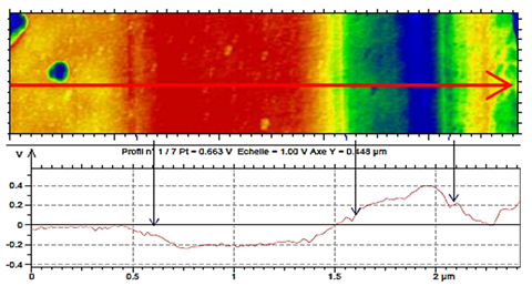
Figure 1. HD-KFM™ surface potential map of a perovskite film and schematic of its cross-section. The high-resolution map reveals distinct domains and variations at grain boundaries, providing critical information on charge separation efficiency and potential loss mechanisms. This level of detail is essential for optimizing cell structure and performance. Image Credit: CSInstruments
ResiScope™: Artifact-Free Conductivity Mapping Across 10 Orders of Magnitude
The Architectural Advantage of DSP Control
ResiScope™'s unique hardware architecture addresses the basic constraints of traditional C-AFM.
Traditional C-AFM systems use a succession of fixed-gain amplifiers that must be manually selected by the user. This method is fundamentally flawed: if the local conductivity is too high for the chosen gain, the signal saturates, and crucial information is lost. If the conductivity is too low, the signal gets lost in the noise.
ResiScope™ replaces the rigid design with an intelligent system managed by a fast Digital Signal Processor (DSP).
The DSP continuously monitors the current signal in real time and, in microseconds, automatically picks the best internal amplifier for that place on the sample.
The Power of a 10-Decade Dynamic Range
ResiScope™'s DSP-controlled architecture allows it to detect resistance from 10² to 10¹² Ω and current from 50 fA to 1 mA in a single scan.
This 10-order-of-magnitude range is critical for photovoltaic materials, which are frequently complex composites of metallic electrodes, semiconducting active layers, and insulating domains.
Source: CSInstruments
| Parameter |
Conventional C-AFM |
ResiScope™ |
| Hardware Architecture |
Fixed-gain amplifiers |
DSP-controlled, multiple internal amplifiers |
| Gain Control |
Manual selection, fixed during scan |
Real-time, auto-ranging adjustment |
| Dynamic Range (single scan) |
Limited (3-4 orders of magnitude) |
Unprecedented (10 orders of magnitude) |
| Current Protection |
Limited or non-existent |
Intelligent, real-time protection |
| Common Artifacts |
Saturation, capacitive effects, slope effects |
Artifact-free measurements |
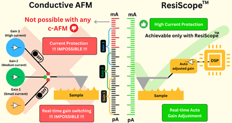
Figure 2. Comparing Conductive AFM (c-AFM) mode with ResiScope™. Image Credit: CSInstruments
Soft ResiScope™: Non-Destructive Electrical Characterization of Delicate Organic Solar Cells
Introducing the 3rd AFM Mode: Soft Intermittent Contact (Soft IC)
Traditional AFM faces a fundamental challenge when characterizing delicate, fragile samples, such as OSC active layers. While Contact Mode provides direct force control, it also subjects the sample to continuous lateral and shear stresses, which can easily cause irreparable damage, such as scratches or material displacement.
Resonant modes (e.g., Tapping Mode) significantly reduce these destructive forces, but they have limited capabilities for quantitative electrical and mechanical measurements.
CSInstruments' solution to this problem is Soft Intermittent Contact (Soft IC) Mode, a true "3rd Mode" of AFM operation.
Its working principle is elegantly simple yet profoundly effective: the AFM tip is brought into contact with the surface using a perfectly controlled constant force, and measurements are taken. The tip is then fully retracted from the surface and moved laterally to the next measurement location.
Soft ResiScope™ for Organic Photovoltaics
Soft ResiScope™, a non-destructive technique for examining fragile organic photovoltaic materials, combines Soft IC Mode's delicacy with ResiScope™'s strong electrical characterization. OSC active layers are notoriously soft, making them easily altered or destroyed by the scraping motion of a standard conductive AFM tip.
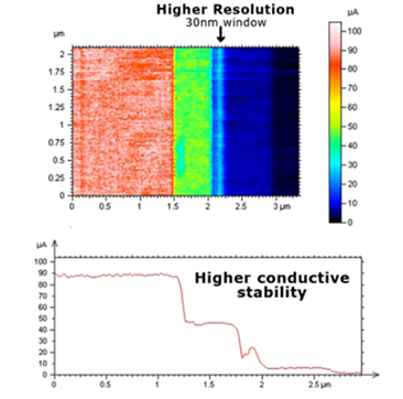
Figure 3. High-resolution (30 nm) ResiScope™ electrical mapping of a BSF silicon solar cell. The image clearly shows the current distribution and the sharp transition at the junction, highlighting the technique's utility for detailed characterization and quality control of semiconductor devices. Image Credit: CSInstruments
Multi-Modal Analysis: Correlating Conductivity, Potential, and Performance
The ultimate power of the CSInstruments platform is the seamless integration of its sophisticated modes.
The Nano-Observer AFM series enables users to transition between Soft ResiScope™ and HD-KFM™ on the same sample region with a single click in the software. There is no need to change the conductive tip, withdraw from the surface, or reposition the device to ensure flawless dataset registration.
Application Showcase: From Organic Blends to Perovskite Grains
Organic Solar Cells (OSCs)
Soft ResiScope™ offers valuable insights in a P3HT/PMMA organic blend. The Soft ResiScope™ current map differentiates the conductive domains of the P3HT polymer from the surrounding insulating PMMA matrix, despite the film's seemingly flat topology.
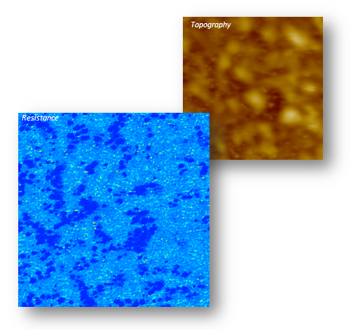
Figure 5. Soft ResiScope™ analysis of a P3HT/PMMA organic solar cell active layer (10x10 µm scan). While the topography (inset) shows little contrast, the current map clearly differentiates the conductive P3HT domains (green) from the less conductive PMMA regions (blue), revealing the nanoscale electrical morphology essential for device performance. Image Credit: CSInstruments
Inorganic Solar Cells
ResiScope™ maps resistance distribution for PSCs, where grain boundaries play a significant role in performance. These maps are important for understanding charge transport efficiency and the significance of ion migration.
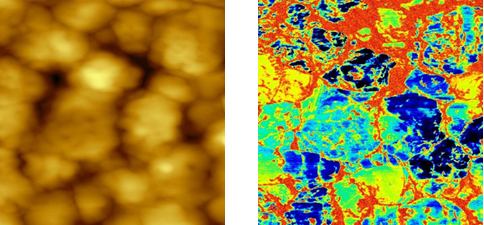
Figure 6. (Left) Topography and (Right) ResiScope™ resistance map of a perovskite solar cell film (2x2 µm scan). The electrical map reveals detailed resistance distribution across 10 orders of magnitude, highlighting variations in conductivity at grain boundaries that are critical for device optimization. Image Credit: CSInstruments
Empowering the Next Wave of Photovoltaic Innovation
CSInstruments' advanced AFM technology addresses the most critical nanoscale characterization challenges in solar research. The technologies described in this article provide distinct and substantial benefits over conventional methods:
- HD-KFM™ offers superior resolution and sensitivity for mapping surface potential and work function, providing valuable insights into the electrical properties of PV materials.
- ResiScope™ provides accurate conductivity measurements across a 10-decade dynamic range, capturing the whole electrical behavior of complicated devices in one pass.
- Soft ResiScope™ enables non-destructive electrical characterization of fragile materials such as organic solar cells, paving the way for new investigations on degradation and stability.
The CSInstruments' Nano-Observer AFM Series transforms the AFM into a powerful diagnostic tool, providing researchers with the critical insights needed to address the most fundamental challenges in photovoltaics and accelerate the development of more efficient, stable, and cost-effective solar energy technologies.

This information has been sourced, reviewed and adapted from materials provided by CSInstruments.
For more information on this source, please visit CSInstruments.