Sponsored by LuxorReviewed by Louis CastelJul 2 2026
Thin films made from materials like gold or platinum, applied through sputter coating, do not always exhibit the familiar "metallic appearance" encountered in daily life. When the thickness of gold or platinum coatings falls below 15 to 20 nm, they fail to display the expected "gold appearance" or "platinum appearance."
Image Credit: Luxor
This phenomenon is frequently misinterpreted by sputter coater operators as an indication that no coating or an inadequate coating has been applied, even though the desired coating is present.
LUXOR conducted an experiment in which gold and platinum of varying thicknesses were deposited onto a stub using carbon tape to clarify this prevalent misconception. The following are the results:
Gold:
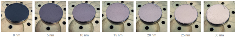
Image Credit: Luxor
Platinum:
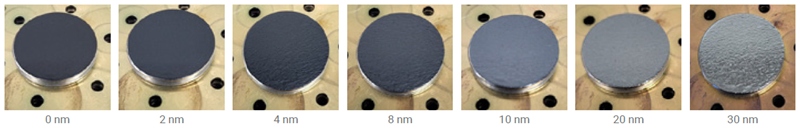
Image Credit: Luxor
It is evident that the characteristic gold or platinum appearance only becomes apparent for layers exceeding a thickness of 20 nm. Layers that are thinner typically exhibit a somewhat reflective or grayish look. Elemental analysis conducted in the electron microscope using EDS confirms the presence of a gold or platinum layer.
From a practical standpoint, it is crucial to recognize that if a distinct gold or platinum layer is observed on the coated sample, it is highly likely that the coating thickness significantly exceeds the conventional 2 nm to 5 nm for platinum or 5 nm to 10 nm for gold, which is necessary to prevent charging in most materials. In such instances, it is advisable to adjust the coater parameters to achieve thinner layers while maintaining the visibility of the sample's topography.
This may seem straightforward, but when using manual coating systems, there is often little control over coating process parameters, leading to coatings that are excessively thick or lack homogeneity. In these situations, employing the aforementioned images as a quick reference can be extremely beneficial in assessing the quality and thickness of the applied coating.
What is Sample Charging?
In an electron microscope, samples are situated within a vacuum chamber and subjected to an electron beam. During this process, non-conductive or weakly conductive samples may accumulate electrical charge, resulting in unusual contrast and 'overexposed' images.
This problem can be alleviated by applying a thin layer of a conductive material, typically gold, platinum, or carbon, to the sample surface. The most prevalent methods for this coating are thermal evaporation for carbon and plasma sputter coating for gold and platinum. This preparation method is commonly known as SEM coating.
Tissue Paper Uncoated (1.000x Magnification)
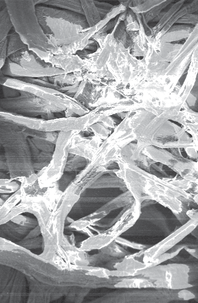
Image Credit: Luxor
Tissue Paper Coated 5 nm Gold Layer (1.000x Magnification)
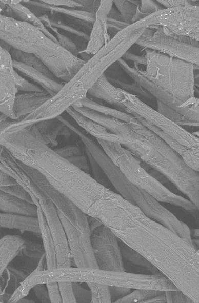
Image Credit: Luxor
Why Choose LUXOR?
A2 Technology: Precision Coating for High-Resolution Imaging
Image Credit: Luxor
LUXOR's distinctive and advanced A2 technology produces plasma with remarkable precision and control, resulting in a consistently thin, uniform coating. The process begins with establishing a vacuum in the chamber, followed by applying a high voltage. To maintain stability, the resulting coating current is automatically adjusted by introducing small quantities of process gas into the reactor, enabling the target current to be achieved and sustained.
What sets LUXOR metal coaters apart from other commercially available devices is the innovative approach employed to manage and modify this process. For operators of scanning electron microscopes (SEM), this translates into acquiring more consistent, uniform metal coatings, which significantly improve image quality by enhancing resolution and contrast. Furthermore, the coating process is entirely automated, eliminating the necessity for manual intervention and providing a smooth and hassle-free experience.
Innovative Upside-Down Design for Greater Functionality
LUXOR embraces a philosophy of 'form follows function,' which is the reason that metal coaters are designed uniquely with samples and targets positioned upside down. Although this may appear unconventional initially, it provides numerous substantial benefits.
All voltage and current wires are safely contained within the sputter device, greatly minimizing the risk of electric shock. This safety feature enables the user to use the machine with total confidence.
The inverted design ensures that the lid, which also serves as a sample loading station, is readily accessible. This feature enables one to apply or remove samples swiftly, eliminating the necessity for specialized tongs or tweezers. Such simplicity not only improves usability but also increases productivity by optimizing the process.
This design guarantees the removal of loose particles during the coating process, thereby aiding in the optimal protection of the Scanning Electron Microscope (SEM) from debris. As a result, this leads to more consistent and dependable outcomes.
Furthermore, larger particles within the plasma are attracted to the pump instead of reaching the samples because of their weight, which leads to enhanced coating quality. This phenomenon, along with the algorithms utilized in the A2 technology, removes the necessity for a rotary or planetary table, significantly streamlining the setup for coating three-dimensional and porous samples.
Fully Automated
The coating procedure is fully automated. After loading the samples, users need to choose the preferred coating thickness and press the start button. This intuitive system significantly minimizes the chances of human error. New operators and laboratory staff can master the operation of the device in just a few minutes of fundamental training.

This information has been sourced, reviewed and adapted from materials provided by Luxor.
For more information on this source, please visit Luxor.