EV Group (EVG), a leading supplier of wafer bonding and lithography equipment for the MEMS, nanotechnology and semiconductor markets, today announced that Himax Technologies, Inc., a leading producer of CMOS image sensors, power management devices and semiconductor devices and components used in flat panel displays, has placed a repeat order for an IQ Aligner UV nanoimprint lithography (UV-NIL) system from EVG.
The IQ Aligner will be used by Himax to support the company's capacity increase in the production of wafer-level cameras used in mobile phones, notebook computers and other consumer electronic devices, as well as to support the increasingly stringent manufacturing requirements for wafer-level cameras demanded by Himax's customer base. The IQ Aligner will be shipped and installed at Himax's manufacturing facility in Tainan, Taiwan.
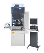 The IQ Aligner UV-NIL System from EV Group.
"EV Group's flexible IQ Aligner platform and the company's microlens molding process expertise are important enablers in achieving higher levels of quality in wafer-level optics while also lowering their cost of production," stated HC Chen, fab director at Himax. "This adds to our already advanced manufacturing capabilities for CMOS image sensors, and provides us with a key competitive edge by enabling us to offer a complete manufacturing solution to the mobile handset market."
Microlenses are an integral component in the optical systems used in wafer-level cameras, and their quality is a critical factor in determining overall product performance. With cost margins extremely tight for the wafer-level camera market, manufacturers need solutions that enable high repeatability and high accuracy. EVG's IQ Aligner is the industry-proven, high-volume manufacturing solution available today for wafer-level optics--which is essential in supporting the production of smaller, higher-performance wafer-level cameras.
"This repeat order from Himax further extends our market and technology leadership in lens molding, with nearly every major wafer-level optics manufacturer having adopted our suite of solutions," stated Paul Lindner, executive technology director, EV Group. "We look forward to working with Himax to ensure their continued success in developing the advanced wafer-level optics that support their customers' leading-edge product roadmaps."