EV Group (EVG), a leading supplier of wafer bonding and lithography equipment for the MEMS, nanotechnology and semiconductor markets, today announced that it has installed a fully automated 300-mm system from EVG's Gemini® product family of integrated wafer bonding clusters to a leading Chinese semiconductor foundry.
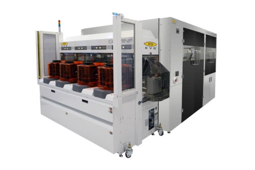 EVG GEMINI(R) Wafer Bonding System. (PRNewsFoto/EV Group
This customer will use the system for 3D IC integration and advanced packaging—two high-volume applications for which EVG's wafer bonding solutions have become the de facto industry standard.
"This order from one of the largest Chinese foundries further cements EV Group's position as the market and technology leader in wafer bonding for leading-edge applications," stated Hermann Waltl , executive sales and customer support director at EV Group. "China is an important market for us, and this order is further testament to our continued success in penetrating leading high-volume microelectronics manufacturers in China—from advanced substrate suppliers to light emitting diode (LED) and semiconductor device makers."
EVG won this order following a competitive bid with other leading process equipment suppliers. Reasons cited by the customer for choosing EVG included high alignment accuracy, comprehensive process development and support, successful demo results in EVG cleanrooms, unmatched expertise in wafer bonding and other high-volume process solutions, and a technology roadmap that is strongly aligned with that of the customer.
The EVG Gemini is a fully automated and integrated platform for wafer conditioning, wafer-to-wafer alignment and wafer bonding. This highly modular design provides customers with a highly flexible solution that can integrate all of EVG's technology solutions in one platform with minimized footprint. Configurations can include the option of EVG's clean modules, low temperature plasma activation modules, SmartView® align modules with integrated bond capability, as well as dedicated bond modules.
EV Group will be exhibiting its technology solutions portfolio at SEMICON China, March 19-21, 2013 in Shanghai.