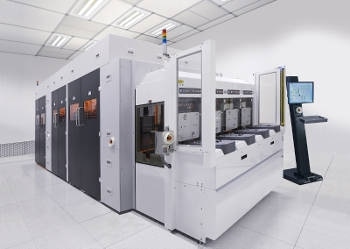
EV Group (EVG), a leading supplier of wafer bonding and lithography equipment for the MEMS, nanotechnology and semiconductor markets, today announced that its EVG GEMINI® 300-mm automated wafer bonding system is ready for implementation into MEMS high-volume manufacturing (HVM).
This marks an important milestone for the MEMS industry, which until now has utilized smaller 200-mm wafer substrates for MEMS HVM. The combination of industry-leading alignment and excellent temperature and pressure uniformity for high-force permanent bonding on EVG's benchmark, production-proven GEMINI 300-mm platform now brings this critical process to 300-mm MEMS manufacturing.
In addition, the ability of the GEMINI wafer bonder to support 300-mm MEMS manufacturing enables more cost-effective implementation of emerging applications, such as CMOS-MEMS integration.
According to market research and strategy consulting firm Yole Développement, the consumer MEMS market is projected to achieve a 12.3 percent compound annual growth rate (CAGR) from 2015 to 2020, with much of this demand being driven by the need for increasingly sophisticated, more numerous and lower-cost bulk acoustic wave (BAW) filters and microphones for smart phones and other mobile electronic devices.*
To support this growing demand, MEMS manufacturers will need to increase their production capacity as well as integrate more complex manufacturing processes in their production flow.
Many MEMS devices have very small moving parts, which must be protected from the ambient environment. High-force permanent wafer bonding allows wafer-level capping of MEMS devices, which seals a wafer's worth of MEMS devices in one operation—after which the capped devices can then be packaged in a much simpler and lower-cost package.
Enabling this process on larger 300-mm substrates, EVG's GEMINI platform allows MEMS manufacturers to increase production yields as well as lower their overall cost of production. At the same time, the GEMINI's ability to perform permanent bonding of 300-mm MEMS wafers allows for CMOS-MEMS integration—the combining of CMOS and MEMS technology to enable more sophisticated integrated MEMS devices—without requiring chip-to-wafer bonding or wire bonding, which can increase production costs or increase the footprint of the MEMS device.
"For more than 15 years, EV Group has revolutionized automated wafer bonding, and established itself as the clear technology and market leader with the largest installed base of automated production wafer bonding systems worldwide," stated Paul Lindner, executive technology director at EV Group.
"Representing the first platform to incorporate all wafer bonding process steps in a single automated system, GEMINI has proven to be one of our most successful products. As part of EVG's Triple-i philosophy, we have continually innovated this product over the years to achieve new levels of capability and performance for our customers, including supporting advanced packaging HVM applications such as CMOS image sensors and 3D-ICs.
"Now, we are bringing the capabilities and success of this versatile platform to our MEMS customers to support their evolving needs—whether it be higher production capacity to meet rising consumer demand, more integrated MEMS systems with improved functionality and accuracy, or new types of devices enabled by CMOS/MEMS integration."
The GEMINI 300-mm automated wafer bonder incorporates many features to enable high throughput, high post-bond yield and low cost of ownership, including:
- EVG's proprietary SmartView®NT automated bond alignment system, which provides sub-micron alignment accuracy and transfer of the aligned wafer pair using proprietary bond chuck technology. This is crucial for ensuring optimal wafer-to-wafer bond yields
- A modular design that allows customers to customize, scale or even reconfigure their systems for different bond processes according to their production needs
- Integrated wafer preparation and conditioning, including oxide removal, which is critical to ensuring maximum bond strength between wafers
- Swap-in modules for rapid changeover and optimum serviceability, depending on bond processes and pre-processing needs
- Ability to handle bond temperatures of up to 500 degrees Celsius and bond forces up to 100 kilonewtons (kN)
- Optimized temperature uniformity as well as controlled rapid heating and cooling capability
Demonstrations of the EVG GEMINI 300-mm wafer bonder for MEMS applications are available at EVG's headquarters in St. Florian, Austria.
* Source: Status of the MEMS Industry 2015, Yole Développement, 2015.
About EV Group (EVG)
EV Group (EVG) is a leading supplier of equipment and process solutions for the manufacture of semiconductors, microelectromechanical systems (MEMS), compound semiconductors, power devices and nanotechnology devices.
Key products include wafer bonding, thin-wafer processing, lithography/nanoimprint lithography (NIL) and metrology equipment, as well as photoresist coaters, cleaners and inspection systems. Founded in 1980, EV Group services and supports an elaborate network of global customers and partners all over the world. More information about EVG is available at www.EVGroup.com.