Image Credits: Bruker Nano Surfaces Division
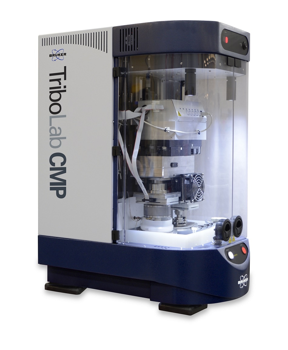
Bruker’s Nano Surfaces Division today announced the introduction of the TriboLab CMP Process and Material Characterization System, which provides a unique characterization capability for the development of chemical mechanical polishing (CMP) processes on the proven robust UMT TriboLab™ mechanical testing platform. The new TriboLab CMP system is the only tool on the market that can provide a broad range of polishing pressure (0.05-50 psi), speeds (1 to 500 rpm), friction, acoustic emissions, and surface temperature measurements for the accurate and complete characterization of CMP processes and consumables.
”CMP is more critical than ever for advanced semiconductor device fabrication. The industry has been calling for a means to effectively characterize the detailed process and consumables interactions that take place while polishing a wide range of materials,” said Dr. Robert Rhoades, CTO of Entrepix, a leading provider of equipment and wafer processing services to the CMP industry. “We are pleased to partner with Bruker and assist in the launch of the TriboLab CMP platform. With the addition of this new system to our capabilities, we are poised to provide a reliable R&D solution for testing and characterization of complex interactions among pads, slurries, conditioning, and process parameters with unmatched repeatability and detail.”
Bruker has supplied instruments for this application for well over a decade, and we are delighted to introduce TriboLab CMP as the latest generation product of this family. TriboLab CMP has already demonstrated superior capabilities at customer sites on some of the most challenging CMP applications development in the semiconductor industry. It is the only tool on the market that can provide the broad polishing pressure and speed ranges, acoustic emission data, friction, and surface temperature for accurate and complete characterization of CMP processes and consumables.
James Earle, Vice President and General Manager, Tribology, Stylus and Optical Metrology Business, Bruker