|
Carbon nanotubes offer a range of attractive properties and could enhance many coatings applications. However, the current barriers to mass-market use of these materials include the availability of high-quality materials in commercial quantities. Now a partnership between industry and academia has resulted in a commercial manufacturing process for carbon nanotubes.
Industry Applications for Carbon Nanotubes
Hardly a day goes by without someone suggesting a new application for carbon nanotubes. Since their discovery, academics and industrialists have researched or considered their use in brake discs; fuel cells; advanced aerospace composites; co-axial cable; conductive fuel lines; EMI (Electromagnetic Interference) shielding in electronic devices; conductive tyres; conductive inks; and, of course, the hotly disputed space elevator – to name but a few. While some of these applications are clearly closer to reality than others, possibly the most immediate products will be developed in the coatings industry. The launch in April 2004 of the UK’s first commercial manufacturing process for high-purity single-wall carbon nanotubes at Thomas Swan & Co. Ltd., has cleared the way for the development of a wide range of advanced coatings applications.
Composition and Classification of Carbon Nanotubes - Single-Wall (SWNT) and Multi-Wall (MWNT)
For those who have not come across them before, carbon nanotubes consist of molecular cylinders of pure, hexagonally-arranged carbon atoms that resemble rolled-up sheets of chicken wire with a diameter measured in a few nanometres (1 nanometre is 1 billionth of a metre) and a length of many microns. They occur in two main types, the single-wall carbon nanotube (SWNT) composed of a single cylinder of carbon (Figure 1), and the multi-wall version (MWNT) (Figure 2) consisting of concentric tubes or cylinders of carbon (effectively straws within straws). The ends of the tubes are usually closed off by a carbon end-cap. Other variations on this theme include the double-wall tube, ‘herringbone’ and ‘bamboo’ structures.
|
|
|
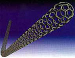
Figure 1. Graphic depicting a single-wall carbon nanotube.
|
|
|
|
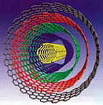
Figure 2. Graphic depicting a multi-wall carbon nanotube.
|
Strength and Properties of Carbon Nanotubes
Since their discovery, and Sumio Iijima’s watershed paper in 1991, there has been unprecedented academic and industrial interest in carbon nanotubes and their potential use in a wide range of commercial applications. There is no denying that the basic properties of both single and multi-wall carbon nanotubes are truly remarkable. Recent studies have suggested that single-wall carbon nanotubes have a tensile strength of 50-100 GPa and a modulus of 1-2 TPa. This places them well ahead of steel in both strength and modulus and all for one sixth the weight. Combine this with their high thermal and electrical conductivity and you begin to understand why so many scientists and commercial organisations have sat up and taken notice.
Properties of the Individual Carbon Nanotube
The basic properties of the individual carbon nanotube (both single and multi-wall) have been considered in some fascinating potential applications. In essence carbon nanotubes are advanced fillers - highly conductive (thermally and electrically), extremely strong and light-weight. Add to this their apparent ability to absorb electro-magnetic interference and the fascinating photo-acoustic effect (whereby they spontaneously ignite when exposed to an intense light source) and you are left with some intriguing possibilities for advanced coatings.
Electrical Conductivity of Carbon Nanotubes
The addition of low concentrations of carbon nanotubes to plastic it makes it electrically conductive. This allows electrostatic painting to be used when coating automotive parts, removing the need for costly primers.
Benefits of Modest Loadings of Single-Wall Carbon Nanotubes
The high aspect ratio of carbon nanotubes (length divided by diameter) means that they form a percolating matrix across the non-conductive filler at much lower loadings than traditional fillers. Carbon black typically requires 30 or 40% by volume loading to confer conductivity, at which point the mechanical properties of the composite are often severely degraded. In comparison Cambridge University recently achieved a conductive epoxy using only 0.005 wt% loading of aligned multi-wall carbon nanotubes. It is also likely that modest loadings of single-wall carbon nanotubes will actually enhance the structural properties of the composite.
Anti-Static Properties of Carbon Nanotubes May Be Used in Packaging for Electronics
The anti-static properties of carbon nanotube coatings may also have potential applications in packaging. Anti-static coatings are used in the electronics to prevent damage to sensitive electronic components during shipping and storage.
Thermal Management Potential of Carbon Nanotubes
Carbon nanotubes (in their pure and undamaged form) are possibly the best thermally conductive material ever discovered. As such they are being researched for their heat management potential in a number of applications. As the electronics world strives to fit more and more functionality into less and less space, overheating is becoming a major problem. This is forcing greater pressure on materials and coatings involved in electronics manufacturing to be thermally conductive in an attempt to remove the heat from the device as quickly as possible.
Low Loadings of Carbon Nanotubes Should Speed Up Curing Times
Another aspect of thermal management is the demand for rapid curing times of polymeric materials such as ink resins and elastomers. The use of low loadings of carbon nanotubes should increase the speed of thermal dissipation from a coating or resin allowing for a much faster curing time. This would clearly be of interest in automated processes where the speed of curing limits the rate of production.
Electrostatic Dissipation Properties of Carbon Nanotube Coatings
Electro-magnetic interference (EMI) shielding in laptops and mobile phones is becoming increasingly important to preventing interference with and from other portable electronic devices. As an extension to the electrostatic dissipation properties of carbon nanotube coatings, a number of companies are developing coatings that are designed to absorb EMI.
Using Carbon Nanotubes in Conductive Inks for Spray-On Circuits and Coatings
A significant amount of research is being directed into the use of carbon nanotubes in conductive inks. The ability to spray on conductive ink opens up some intriguing possibilities for ‘spray-on’ circuits and coatings. A leader in this field is US-based Eikos which was awarded USD 860,000 in May this year from the US Air Force Research Laboratory to develop transparent conductive polymers specifically for military aircraft canopies.
While such contracts indicate that the carbon nanotube market is already up and running in some niche applications, there are still some major barriers to overcome.
The Three Main Restrictions in the Market-Place for Carbon Nanotubes
While there are already some products in the market-place and a whole range of applications in development, the carbon nanotube market has been constrained by three main issues:
- A lack of commercially-available material of consistently high quality.
- Cost - until recently single-wall carbon nanotubes were selling for EUR 400/g which is clearly some way from commercial viability as a bulk material.
- Successfully expressing the basic properties of the raw material in the end application – the incredibly small scale of the material poses some interesting challenges for advanced material and coatings science.
Such teething problems are not new. Carbon fibres took many years to be widely accepted in the materials world from both a cost and performance aspect and have only just made a regular appearance in popular sporting markets such as golf equipment.
Early Applications of Carbon Nanotubes now on the Market
Despite this, some early applications of carbon nanotubes in products such as conductive fuel lines in the automotive industry have already made a successful appearance on the market. In addition, recent advances in the manufacture of carbon nanotubes on an industrial scale will allow vital commercial research and evaluation to be conducted and this will open the way to a wide range of fully industrialised applications.
The UK’s First Production Plant for Single-Wall Carbon Nanotubes (SWNTs)
The UK’s first commercial manufacturing process for high-purity single-wall carbon nanotubes was announced by Thomas Swan & Co in April 2004. The plant is the result of four years of collaboration between Thomas Swan and Cambridge University’s Department of Material Science and Department of Chemistry. The unique collaboration brought the academic expertise of Cambridge University together with over 77 years of chemical manufacturing experience from Thomas Swan.
Problems Encountered When Setting Up this Plant for Carbon Nanotubes
The goal of the project was to supply high-purity single and multi-wall carbon nanotubes in commercial quantities and to back up this initial offering with the ability to scale up the process to keep up with demand as the industrial market expanded. The problem was that at the start of the programme no-one knew which production method would supply both single and multi-wall tubes and be fully scalable. It was this problem that was presented to Cambridge University.
Different Methods Used for Manufacturing Carbon Nanotubes
Carbon nanotubes can be manufactured using a variety of methods:
- Laser ablation uses a high-power laser to vaporise a graphite source loaded with a metal catalyst. The carbon in the graphite reforms as predominantly single-wall nanotubes on the metal catalyst particles.
- Arc discharge involves an electrical discharge from a carbon-based electrode in a suitable atmosphere to produce both single and multi-wall tubes of high quality but in low quantities.
- Chemical vapour deposition (CVD) is where a hydrocarbon feedstock is reacted with a suitable metal-based catalyst in a hot furnace to ‘grow’ nanotubes which are subsequently removed from the substrate and catalyst by a simple acid wash.
Using a System Based on Chemical Vapour Deposition (CVD) Growth
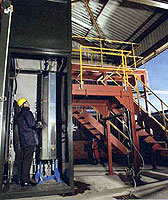
The team at Cambridge developed a novel system based on CVD growth, as it enabled the production of both single and multi-wall nanotubes of reasonably high quality and consistency while offering the greatest potential for scale up. This concept was then taken to design stage (and patented by Cambridge University). Using a team of chemical engineers and an independent consultant, the plant was built at Swan’s site in North East England towards the end of 2003 (Figure 3). Over the following months the plant was commissioned and then optimised until the material that was being produced was of consistently high quality.
|
|
|
Figure 3. Photo showing the Swan nanotube plant in Consett, County Durham.
|
Benefits of Having Access to a Regular Supply of High-Purity and Scaleable Material
A consistent supply of high-purity material that is also scaleable is a major stepping stone for the developing carbon nanotubes market. It allows companies to conduct meaningful industrial research using commercial quantities of raw material. In addition, this research can now be done with the knowledge that, should an application prove itself, there is a scalable source of the same raw material available to supply any ongoing development. Combine this with lowering prices (Thomas Swan predicts that within a few years the price of single-wall carbon nanotubes with be measured in tens of GBP per kg) and the market should start to take off.
Problems in Seeing What has been Manufactured
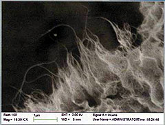
A major problem in achieving a saleable product that is on average 100,000 times smaller than a human hair is that it is rather hard to ‘see’ what you have made. The advent of nanomaterial manufacturing brings to light the necessity for advanced industrial and cost-effective analytical techniques. While Scanning Electron Microscopes (SEM) provide the ability to view the sample in remarkable detail, it only shows a minute fraction of the product (Figure 4). The analogy often used is like looking at a football pitch through a jam jar. The grass beneath you is green and healthy but you have no idea what it is like on the other side of the pitch.
|
|
|
Figure 4. Scanning Electron Micrograph (SEM) of Elicarb SW high-purity single-wall carbon nanotubes.
|
Tools and Techniques Used to Help Manufacturers See what they are Making
This will not be an easy problem to solve and while RAMAN techniques (which involve studying the spectrum profile of a reflected laser from your sample) offer some hope, it will be some time before a standard industry protocol for purity measurement is identified and accepted. Thomas Swan currently bases purity measurement on a combination of SEM, (Transmission Electron Microscopy) TEM, RAMAN and Thermal Gravimetry Analysis (TGA) techniques, combined with an experienced technical eye and has so far received very encouraging feedback from early customers. As the company moves to scale the process up, ongoing customer feedback and collaboration will become increasingly vital.
Prices of Carbon Nanotubes Will Fall as Demand Increases
Carbon nanotubes are still in the very early stages of industrial development. While they are still expensive compared to a fully commoditised product, such as carbon black, the price will fall as the demand increases. Despite the problems associated with analysis and downstream processing (namely dispersion) the basic properties of the raw material offer a wide range of exciting applications that are beginning to be realised.
What the Next Ten Years Might Hold for Producers of Carbon Nanotubes
As the research into these applications moves out of the lab and into industry it is important that the supply of carbon nanotubes is consistent, of high quality and performed under the appropriate regulatory and health and safety protocols. Thomas Swan has taken the first step towards this goal and material is now available to allow meaningful industrial evaluation and development. The next ten years of development should see the creation of a whole new area of material and coatings science and associated commercial applications.
|