|
The kSA MOS Ultra-Scan is a flexible, high-resolution scanning curvature and stress measurement system. Based on proven kSA MOS technology, this fully integrated ex-situ tool maps the curvature of semiconductor wafers, optical mirrors, lenses, or practically any polished surface. The kSA MOS Ultra-Scan measures stress by monitoring wafer curvature with an array of parallel laser beams and a CCD area detector. Optimized optics and detection system combined with proven fitting algorithms result in typical radius of curvature resolution greater than 50 kilometers. Scans are fully programmable for selected area, line scan, or full area map. The kSA MOS Ultra-Scan also provides quantitative film stress with full area map for 50-200mm wafers by first scanning the bare substrate and then re-scanning the sample post-process.
The kSA MOS Ultra-Scan offers 10x higher stress resolution, lower noise, and more powerful mapping capabilities than any other system available. Applications include non-lattice matched compound semiconductor deposition, Silicon on Insulator (SOI) and strained silicon substrates, or any polished surface where 2D curvature and stress are desired. Samples are manually loaded onto the xy stage for scanning.
Figure 1. kSA MOS Ultra-Scan
kSA Multi-beam Optical Sensor
The only commercial in situ stress monitoring system proven for thin-film deposition The kSA Multi-beam Optical Sensor (MOS) is a thin-film stress, wafer curvature, and thickness measurement tool with integrated real-time feedback for process control. This laser based system is highly sensitive and is proven to be extremely robust. With optimized optics and detection system capturing an array of reflecting parallel laser beams, MOS uses proven fitting algorithms to measure a radius of- curvature between 4 and 10 kilometers (depending on system geometry). Because the technique is optically based, it is compatible with harsh environments. MOS is ideally suited for real-time feedback to process control systems in the production or research environment.
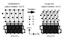 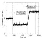
Figure 2. Total stress induced during mismatched metal oxide growth on Silicon during CVD deposition
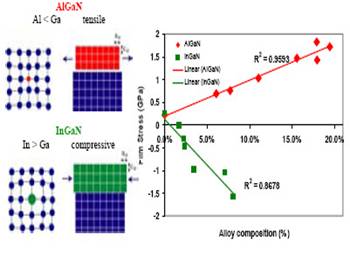
Figure 3. Lattice stress induced during GaN growth. AlGaN growth yields increasing tensile strain with Al content, while increasing In content creates compressive strain.
Features
• Patented, high resolution multi-beam optical technique
• Virtually immune to vibration
• Two port or single port, normal incidence
• Integrated real-time feedback
Benefits
• Real-time analysis of 2D thin-film stress
• Evolution of strain during thermal cycling, buffer layer, and active layer growth
• Strain engineering to improve device performance
• Optional real time thickness, growth rate, and optical constant (n, k) determination
How It Works
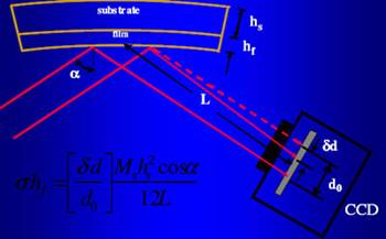
Figure 4 Stress in thin films induces curvature in the substrate. The kSA MOS system measures the curvature optically by monitoring the deflection of parallel beams of light.
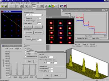
Figure 5. Powerful analysis software
Patented Multibeam Optical Technology
Laser array directly measures stress induced curvature without using rotating mirrors or complex optics.
A single laser is used to generate a two-dimensional array. Changes in the beam spacing are used to determine curvature and subsequent induced stress. Beam intensity variations may be used to determine growth rate and optical constants (n,k).
The ability to directly image and view the entire reflected laser array greatly simplifies use and alignment compared with other position-sensitive detectors. Simultaneous detection of the array makes the measurement inherently less sensitive to sample vibration compared with scanning-laser systems because all the laser spots move together at the same frequency. So movement or tilt is not detected as a change of curvature. Through the use of simple image processing and data analysis algorithms, MOS can easily detect micron-sized changes in spot position. Such sensitivity enables the system to detect each monolayer deposited on the substrate surface. By monitoring the entire array of beams, spatially varying curvature and stress profiles are obtained with the speed necessary for realtime measurement and process control.
|