Silicon is both a physically interesting and technologically important material having a plethora of applications. There has been great interest in recent years in phase transformations that it undergoes during indentation.
Previous studies have shown that semiconducting Si-I transforms to a metallic state of Si (Si-II) when subjected to local pressures above 11 GPa. This metallic state is not stable at ambient pressures and undergoes a series of further structural transformations as the pressure is released. Although many studies have been reported on these phase transformations, the driving mechanisms and phase transformation pathways are still relatively poorly understood. Exsitu characterization techniques such as Raman micro-spectroscopy and transmission electron microscopy (TEM) allow only the final structure to be analyzed with measurements being extremely difficult at the nanoscale. In-situ electrical characterization is a means to track phase changes during indentation and is proving to be a promising route to understanding the sequence of structural transformations. Here we report on in-situ electrical measurements during nanoindentation of silicon using the Hysitron nanoECR™ system.
Nanoindentation is performed using a Hysitron TriboIndenter® equipped with a modified transducer and a conducting doped diamond tip.
During testing, a voltage is applied to the sample via a conducting stage and the resultant current flow through the sample measured through the conducting tip. This voltage and current measurement is done using a Keithley 6487 picoammeter/voltage source.
Measurements
Measurements are made in two modes: one is to monitor the current through the sample/tip system during indentation whilst a fixed voltage is applied to the sample/stage and second is to sweep the voltage signal to acquire an I-V curve.
Figure 1 shows current-time data (with the corresponding load/unload curve) acquired during indentation in crystalline silicon with an applied bias of +1 V.
The dominant resistance in the circuit is that of the tip/silicon contact which is dependent on the state of the silicon immediately under the indenter tip. An immediate increase in current is observed due to the phase transformation to a metallic state (Si-II) induced by the sharp Berkovich tip and continues to increase with load as the contact area of transformation increases.
The electrical measurements also show sensitivity to features on the unloading curve. Note the increase in current observed on the “popout” event (which is caused by sudden decrease in density and is associated with the formation of Si- III/XII) indicating a sharp drop in resistance of the tip/sample contact and/or the phase transformed material.
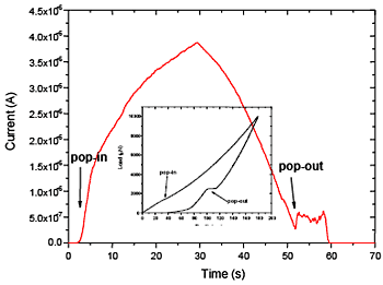
Figure 1. Current versus time curve for a nanoindentation in crystalline Si (100) with a bias of +1 V applied to the sample/stage. Shown also is the corresponding load/unload curve. Current increase is observed immediately on loading and sensitivity to the “pop-out” event is observed on unloading.
By measuring I-V characteristics at different points during a load/unload cycle it is possible to track the changes in the tip/sample contact and therefore of the indented material. Figure 2 shows a set of I-V curves taken at different loads during indentation. On loading the I-V characteristics become more ohmic (characteristic of a tip/metallic Si-II contact) from the initial rectifying curve (tip/crystalline Si-I contact). While during pressure release the I-V characteristic rapidly becomes rectifying indicating phase transformations to a-Si and/or Si-III/XII at the periphery of the Si-II volume created during loading.
The system can be further used as an electrical point probe by applying very low loads (< 100μN - ensuring no plastic deformation) and measuring I-V characteristics.
Figure 3 shows I-V curves measured pre- and post-indentation in this way.
The system not only exhibits high sensitivity to indentation-induced phase transformations but also to variations in the final composition of the indented volume. In the regime of unloading for the data shown in fig. 3, TEM and Raman spectroscopy previously have not shown clear differences in the final structure.
Phase Transformations
The nanoECR system provides a sensitive in-situ means to probe the series of phase transformations silicon undergoes during nanoindentation. Structural changes including phase transformations can be tracked during indentation via current-time as well as I-V curves. Changes in the electrical signature are observed immediately on commencement of loading as well as large changes on unloading coincident with features such as “pop-out” events on the load/unload curve.
Using the indenter as a point probe, post-indentation structure can be measured with very high sensitivity. Correlating such electrical data with the structural information obtained simultaneously from nanoindentation curves provides a powerful new analysis technique.
Although we report on measurements in silicon here, electrical characteristics can be extracted from many other materials systems providing a huge application base.
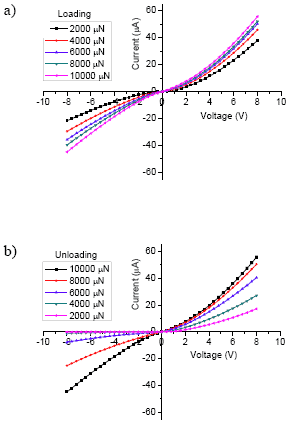
Figure 2. a) I-V curves extracted during loading to 10000 μN in crystalline Si. b) I-V curves extracted during unloading.
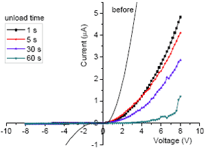
Figure 3. Post-indentation I-V characteristics extracted by holding at 100 μN following unloading at different rates from a maximum load of 10000 μN. Also shown is the I-V characteristic before indentation commenced.
.jpg)
This information has been sourced, reviewed and adapted from materials provided by Bruker Nano Surfaces.
For more information on this source, please visit Bruker Nano Surfaces.