The two-dimensional electronic properties of graphene presents the potential for it to function as a conductor, a transistor, a quantum dot, a molecular switch, or other devices. Since graphene shows weak binding out of plane, the conduction is essentially two dimensional whether the graphene is in contact with a substrate or suspended in free space. Lateral confinement of the conduction path is necessary to engineer these properties. One potentially important confinement is the semiconducting nanoribbon. As the ribbon width decreases below 20 nm, the bandgap increases above the room temperature thermal energy, which opens the door for the production of transistors with high on-off current ratios.
Challenge
A method is needed to create ribbons narrow enough to create the quantum confinement that yields the desired bandgap. There are drawbacks, however, to many of the techniques used to pattern graphene into nano-ribbons. Resist-based lithography has only demonstrated ribbon creation down to a few tens of nanometers in width. This process also leaves residues on the graphene that cause it to ripple, requiring an extra cleaning step. This method is not viable on freestanding graphene, either. Scanning probe methods, while offering high spatial resolution, are slow - and they also cannot be used on freestanding graphene. Ion milling with traditional LMIS-based FIB has not been able to create narrow enough structures and also creates significant damage to the layer.
ORION® PLUS Solution
Helium ion microscopy (HIM) offers the ability to carry out both high precision ion machining and sub-nanometer resolution imaging with high surface sensitivity in order to inspect patterns created in graphene. Nano-ribbons can be machined narrow enough to get deep into the quantum confinement regime and also maintain very long aspect ratios. The dose to mill through graphene is two orders of magnitude higher than that needed for a typical image, so it is possible to non-destructively image a graphene-based system directly in the microscope before and after patterning. Simple milling patterns can be created with the ORION® PLUS software interface; for more complex strategies, a lithography pattern generator can be given control of the beam steering. We illustrate these capabilities below by highlighting HIM research that has been carried out.
ORION® PLUS
Nano-ribbon fabrication has been carried out by Dr. Daniel Pickard at the National University of Singapore. To have access to suspended graphene, a silicon wafer with 300 nm of surface oxide was utilized, into which had been etched an array of 3 µm diameter recesses. Graphitic platelets down to single layer thickness (i.e. graphene) were deposited by the exfoliation method. Optical interference was used to determine the layer count and particularly to identify graphene areas. Direct ion beam writing of the nano-ribbons was accomplished by addressing the helium beam, typically at 30 keV beam energy, with a Nanometer Pattern Generation System (NPGS, from JC Nabity Lithography Systems, Bozeman, Montana).
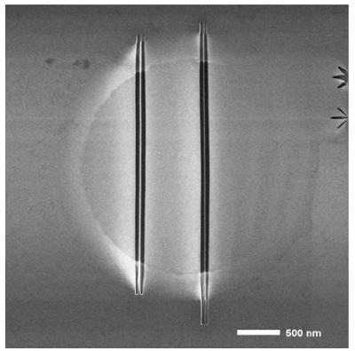
Figure 1. Suspended nano-ribbons created by helium ion milling. Left: 20 nm wide. Right: 10 nm wide.
Figure 1 visualizes the system and shows the results of two nano-ribbon fabrications. The image is a top-down view of one of the recesses in the substrate, covered in this case with 1-3 layers of graphene. On the left a 300 nm long ribbon has been created, with 220 nm of its length suspended over the recess. Its width was programmed to be 20 nm, giving a suspended aspect ratio of 11:1. The programmed width is in accord with the full width at half maximum of the gray level observed in the image. The ribbon on the right is 350 nm long, with 240 nm suspended. Its width is 10 nm, giving a suspended aspect ratio of 24:1. Very conveniently, the structures created can be imaged with good signal by the same beam used to machine them. The strong surface signal from the microscope is confirmed by the observation that the platelet is almost opaque at this thickness. The contrast level between the suspended portion of the ribbon and that over the substrate is just 17 %. With the ability to create such long structures, it is possible then to pattern a nano-ribbon between source and drain contacts to make a functional test device.
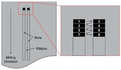
Figure 2. Cartoon representation of the nano-ribbon milling strategy.
The two facets of the process for machining are the ion milling strategy and dose control. For the milling strategy it was found to be critical to minimize any lateral stress on the ribbons during their formation. The nano-ribbon is formed by the creation of two slots, illustrated in the cartoon of Figure 2. The chosen slot width depends on the width and length of the ribbon design but has been demonstrated down to 5 nm wide. If one slot is being milled after completion of the other, the ribbon breaks. Therefore the milling must proceed by applying the entire dose to opposing segments in each slot. Then the beam is directed to the next slice. The order is illustrated by the numerical labels in Figure 2.
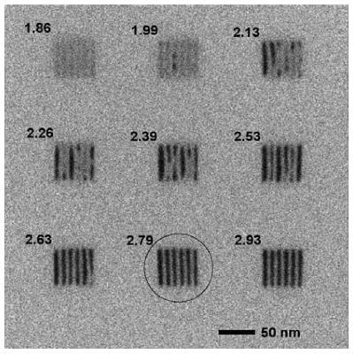
Figure 3. Machining series for the determination of ion dose needed to create nano-ribbons. Dose indicated by each sample, in units of 1018 ions/cm2
.
The second aspect of process control is applied dose. This is determined experimentally. A dose series is shown in Figure 3. A set of ribbon "combs" is milled, each comb at an incrementally higher dose. In the figure, the dose (×1018 ions/cm2) is indicated next to each comb. In this case, 2.79×10¹⁸ ions/cm2 is required to clear the comb completely. This structure can be created in under 10 seconds.
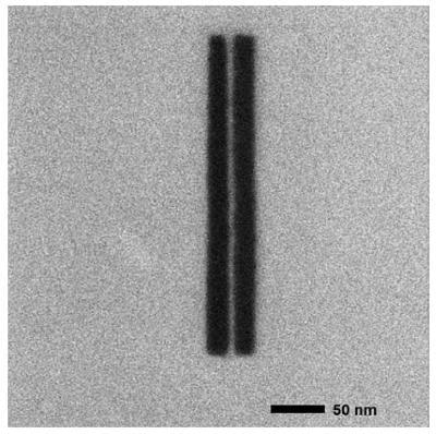
Figure 4. A 5 nm wide ribbon machined in suspended graphene with a 60:1 aspect ratio.
Once the machining strategy is defined, the milling precision can be further explored. Figure 4 shows a nanoribbon just 5 nm wide with an aspect ratio of 60:1 created by this method. Due to the high strength of graphene, more complex shapes can be created as well.
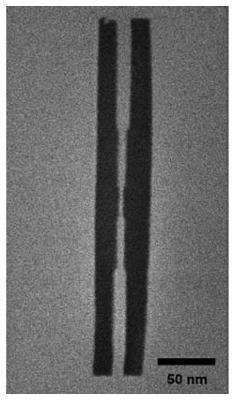
Figure 5. A nano-ribbon machined to have stepped width.
In Figure 5 a ribbon with variable width has been fabricated. The segments near the end measure at 20 nm, then the width steps down to 10 nm and finally to 5 nm at the center. This makes it possible to machine structures defined to express different behaviors. If the orientation of the graphene is known, ribbons with either the "armchair" or "zigzag" orientation can be produced. Devices for researching the creation of quantum dots could be made by having a locally wide area in a narrow ribbon. Any arbitrary electron transport structure can be machined at high speed, with high spatial resolution, and offering immediate inspection capabilities. While this application note focused on suspended graphene, milling has also been demonstrated for graphene directly on a substrate.
ORION® PLUS Capabilities
Nanometer precision ion milling, high spatial resolution imaging which also emphasizes surface detail, use of a non-contaminating ion species; lithographic pattern tool interfacing.
Application
Patterning and inspection of graphene layers with nanometer- scale features for direct-write device fabrication.

This information has been sourced, reviewed and adapted from materials provided by Carl Zeiss.
For more information on this source, please visit Carl Zeiss.