Printed electronics are made of electronic components which can be processed in the form of a liquid solution, and printed onto a substrate in the same way ink is printed onto paper. Whilst the concept has been around for some time, the materials and techniques developed by research into nanotechnology is making flexible circuits more of a commercial reality.
The materials used to form the resistors, capacitors, and other components in a printed circuit can include semiconducting organic compounds, metal nanoparticles, and carbon nanotubes - ongoing research is uncovering more materials which can be used to make printable electronics components every year.
The substrates used to print electronic circuits are usually silicon, glass, ceramics, or polymer films. Polymer substrates have received the most attention recently, as they allow circuits to be made flexible, opening up a fascinating range of new applications.
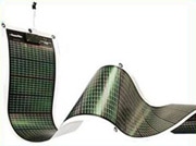 |
| Figure 1. Flexible printed circuits could be used to add smart functionality to everyday objects. Image credit: ORNL.gov |
Benefits of Printed Electronics
Printing electronic circuits, rather than using traditional microfabrication techniques like vapour deposition and etching, provides many advantages, both in terms of the potential applications which are opened up, and during the manufacturing process itself.
Fabrication of printed microelectronics can be achieved using techniques which are very familiar to the graphics printing industry. Roll-to-roll and sheet-fed methods are both possible. Start-up costs are greatly reduced, and short runs of custom products can be accommodated much more easily.
The operating temperatures are also much lower than conventional microfabrication techniques, reducing the energy associated with electronic products.
Electronic circuits manufactured using these techniques are unlikely to be suitable for high-performance applications, where powerful computing or high tolerance to temperature is required.
They will, however, open up a whole new area of low-powered, low-cost applications. Flexible electronics will be able to add "smart" functionality to packaging, labelling and garments. There is also much interest in using them for displays, from large billboard-like screens to portable flexible screens which can be read like a newspaper.
Materials Used in Printed Electronics
Table 1. Materials used for printable electronic components
| |
Material |
Example |
| Conductors |
Conducting polymers |
Polythiophenes, polycarbazoles |
| Metal flakes |
Silver, silver alloys |
| Metal nanoparticles |
Copper, Gold, Silver |
| Carbon nanotubes |
- - - |
| Capacitors |
Inorganic oxides |
HfO2, TiO2, ZrO2 |
| Polymers |
Imide-Norbornene copolymer |
| Organic/inorganic composites |
Metal oxide/epoxy |
| Resistors |
Carbon films |
- - - |
| Optical materials |
RFID antennae |
Aluminium |
| Organic LEDs |
- - - |
Fabrication Methods for Printed Electronics
Roll-to-Roll Printing
Flexographic printing is affordable to set up, due to the use of cheap polymer plates. However, these are not always compatible with the novel inks used for printed electronics.
Gravure printing is highly flexible - it can print layers across a wide range of thicknesses, from 5µm right down to 50nm. The available resolution is also very high, allowing dense circuits to be printed.
Offset printing is well suited to more demanding applications, as it allows a high degree of control, supports a relatively high resolution, and is suitable for rapid production on a large scale. The start-up cost is higher than other methods, however, and a significant volume of waste is produced.
Sheet-Fed Printing
Inkjet printing is the most common and widespread of these technologies. Because of the robust understanding we have of it, it can be adapted to work with a wide range of substrates and inks. It is also much cheaper than the more specialist, advanced techniques listed here. However, it is not clear yet how well it will scale-up to large manufacturing operations. It is likely that inkjet printing electronics will remain dominant for short-run, on-demand applications.
Screen printing is the most mature printing technique for electronics. It is cheap and adaptable, but suffers from relatively thick layer thickness (>20µm) and limited resolution.
Challenges
The most significant challenge for printed electronics is the development and optimization of the materials used. Only a handful of potential substrates have been explored so far, and whilst researchers are discovering nanomaterials with potentially useful electronic properties, there is still a way to go in formulating these into commercial, printable inks.
The manufacturing processes for printing electronics will also require significant development. A few companies are beginning to commercialize the printing of simple electronic systems, but the processes will have to be improved considerably before we are capable of printing complex circuits.
Many commentators believe that the most successful applications of printed electronics will be in hybrid processes, combining printing techniques with established processes like nanoimprint lithography, which is used to create the latest generations of microprocessors. This type of method could provide a reliable, cheaper way to produce electronic components and circuit features on a scale of just a few nanometres, which will be invaluable as our demands on computing equipment escalate.
Conclusion
Printed electronics will have implications across a wide range of industries. Displays, RFIDs, sensors, and wearable or biocompatible electronic equipment are amongst the hottest research topics.
There is also a clear path to commercialization for this technology. Whilst there is still development work to be done, the ubiquity of large-scale techniques for regular printing means that the transition to commercial scale production should be smoother than for most burgeoning nanotechnology products.
References