Introduction
Graphene first burst onto the scientific scene when it was introduced to the world by Geim and Novoselov in 2004, who isolated it in monolayer form using graphite as the base material. The concept itself was much older, having been theoretically established in the 1940s and even named in 1962, by Hanns-Peter Boehm. The discovery fulfilled the predictions and also showed that this material had many other properties that were previously unknown. Its potential applications and uses in both the theoretical and practical fields include electrochemical, biomedical, and optoelectronic , which led to an explosion of interest in 2D materials.
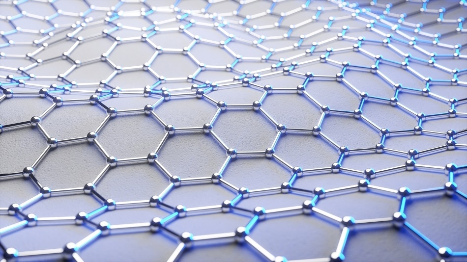
Shutterstock.com/OliveTree
Related 2D materials
Many 2D materials have now been theoretically or practically explored. These all show strange new properties when they are incredibly thin, to the point that they may be considered to be 2D, which are completely different from those of the bulk material. They may be categorized as graphene-related compounds, X-ane compounds and van der Waals (vdW) heterostructures.
- Graphene-related compounds contain the –ene suffix, and include graphene and other related materials, including chlorinated and fluorinated X-enes.
- Compounds whose names end in –ane or in –ide, including the X-anes, carbonitrides and boron nitride.
- The vdW heterostructures, which include the
- MXenes (M being a metal like scandium, hafnium or titanium)
- SMCs (semimetal chalcogenides such as gallium selenide or indium sulfide)
- TMDs (transitional metal dichalcogenides, meaning metal atoms from groups V to VII forming compounds such as MoSe2 and WTe2
- TMCs (transition metal chalcogenides such as III-V and IV-IV complexes )
These may be layered on each other to attempt to tailor their properties for a specific use or property.
1.Graphene
Composed of van der Waal layers of carbon sheets one to a few atoms in thickness, graphene is very stable, is optically transparent, and the strongest of materials. It has excellent carrier mobility and low Joule effect losses. However, the lack of a band gap means it cannot be used for digital circuits as a field effect transistor (FET).
Graphene-related compounds include graphane, graphone, graphyne, graphdiyne, fluorographene, and graphXene. The term graphene itself includes a variety of structures, such as single-layer graphene (SLG), graphene oxide (GO), graphene nanoplatelets (GNPs), and reduced graphene oxide ((RGO). Each has potential for nanoelectronics and spintronics applications.
Graphdiyne can be doped with boron nitride to customize its band gap size. Replacement of carbon with boron nitride leads to the production of a novel material called BNdiyne with an insulating band gap.
GraphXenes are materials produced by various combinations of group IA and VIIA elements which have band gaps in a range between 0 and 6.4 eV, giving the compounds metallic, semiconducting or insulating properties.
2.Elemental 2D compounds
Elemental 2D compounds include monolayers of boron, silicon, germanium, phosphorus, arsenic and antimony, which are called borenene, silicene, silicane, germanene, germanane, phosphorene, arsenene, and antimonene respectively.
Silicene and silicane
Silicene is a crystalline silicon allotrope in 2D form, and has a honeycomb structure of hexagonal units of silicon atoms, like graphene, but with a buckled arrangement. This gives it a larger spin-orbit coupling than graphene, and it can also be used in silicon-based electronic applications more easily than graphene. Many of its properties are tunable by various changes in the atomic arrangement, the type of applied electric field and changes in temperature. Silicene can be used for the same wide range of applications as graphene, including electronic, photonic, magnetic semiconductors, and lithium battery electrodes.
Silicane is silicene modified by bonding one hydrogen atom to each silicon atom, and thus possesses an indirect band gap, at 2-4 eV. It can be used in polariton lasers and optical switches to study excitonic effects, its excitons having high binding energies.
Germanene and germanane
Germanene is composed of a monolayer of germanium deposited on a substrate of gold, or sometimes other materials, in a high-vacuum environment. It has only an indirect band gap and so acts as a semiconductor. A high direct band gap can be created by hydrogenating it to form germanane, leading to a Ge-H bond at each atom, which makes it suitable for optoelectronic uses. Its properties can be tuned by applying a vertical electrical field, and it can be used in many electronic devices. Both silicane and germanane are more stable with respect to thermodynamic properties than graphane.
Stanene and stanane
Stanene is a tin allotrope with a monolayer of tin atoms, and acts as an insulator. Its band gap is inverted and changes with compression. Doping with magnetic materials and electrical gating are both known to change its properties, and it can even become a phonon-mediated superconductor if doped with calcium or lithium or both at extremely low transition temperatures below 1.3 K. Hydrogenation of 2D stanene creates stanane which has a tunable band gap and ferromagnetic behavior at room temperature.
Phosphorene
Phosphorene is a phosphorus allotrope which has a band gap and highly mobile electrons, leading to superior applicability in electronics compared to graphene. In nanoribbon form it has metallic behavior. The band gap value is tunable by compressive or tensile strain or by an electric field in the plane of the sheet. It is photoluminescent, has a very stable structure, and high specific capacity and conductivity to electric current. It has a plethora of uses in batteries, gas sensors, FETs, and radio receivers.
Arsenene
Arsenene is an arsenic allotrope with a graphene-like monolayer of atoms, and absorbs other light atoms such as B, C, N or F to change its magnetic properties . The edge shape can be modified to obtain armchair or zigzag nanoribbons with large indirect and small direct band gaps respectively. On tensile strain the band gap becomes indirect (and smaller), which makes it valuable in LEDs (light-emitting diodes) and solar cells. Compression, on the other hand, first enhances and then reduces the band gap for both monolayer and bilayer arsenene sheets.
Antimonene
Antimonene has two hexagonal lattice forms, alpha (puckered) and beta (buckled), both of which are semiconductors, with indirect band gaps that change with edge shape. Tensile strain causes indirect-to-direct band gap change, as with arsenene. It can be tuned to become a topological insulator at large tensile strain, which makes it useful for ultra-low power electronic devices.
Borophene
Borophene is composed of icosahedral boron atoms that form supericosahedral units, with a six-sided hole in the middle that allow tuning of the chemical and optoelectronic attributes. Borophene has both metallic (though highly anisotropic) and semiconducting attributes, as well as the highest tensile strength of all known structures. Its excellent stability is increased by the presence of vacancies or distortions. It could well be the future material of choice for photovoltaic cells and batteries.
Compounds: hBN, TMDs, and MXenes
Hydrogenated boron nitride
Hydrogenated boron nitride (hBN) has a large band gap of 6 eV which makes it an ideal dielectric for the electrostatic gating of other 2D materials, such as a protective covering, tunnel barrier and gate dielectric, since lattice matching is not needed to form vdW structures. Its structure comprises alternating boron and nitrogen atoms. Its properties are tuned by varying the external electric field, or the thickness of the hBN layer, or by partial oxidation.
Transition metal chalcogenides (TMCs) and dichalcogenides (TMDs)
The TMDs and TMCs have a sheet of transition metal atoms M sandwiched between two hexagonal sheets of chalcogen atoms X (sulfur, selenium or tellurium). The metal atoms are from group IV, V or VI. The structure is rhombohedral or hexagonal, with octahedral or trigonal prismatic coordinate bonds between metal and chalcogen atoms. Multiple layers are linked by vdW forces.
MoS2 is a typical dichalcogenide with a tunable direct band gap in a monolayer. It is used to sense chemicals and gas at very low (ppb) concentrations, as well as in energy storage and collection, flexible electronics and electrochemical catalysis, as well as in emitters (LEDs) and photodetectors. WS2 is another TMC with an optical band gap and high electrical conductivity. They absorb solar radiation because of the vdW forces among the monolayers, and can thus be incorporated into solar cells as semiconductors.
3.vdW heterostructures
TMDs such as WSe2 and MoSe2 can be stacked vertically or linked to other 2D materials to form vdW heterostructures that are polarizable by light, have tunable photonic energy (due to spin-orbit coupling) and valley-specific excitons, making them useful in optoelectronics. They also show conductive, semiconductor, semimetal, dielectric and superconducting properties. The band gaps of various TMDs vary from ultraviolet to infrared range. Their stability makes them suitable for FETs. Tunnel FETs are being built to design p-n junctions made of TMC monolayers in order to bring out logic devices that run on very low power. Other applications include those that deal with energy conversion and storage.
Sources
- https://assets.publishing.service.gov.uk/government/uploads/system/uploads/attachment_data/file/627145/Summary_of_Graphene__and_Related_Compounds__Chemical_and_Physical_Properties.pdf
- https://www.intechopen.com/books/two-dimensional-materials-synthesis-characterization-and-potential-applications/graphene-against-other-two-dimensional-materials-a-comparative-study-on-the-basis-of-electronic-appl
- https://cen.acs.org/articles/95/i22/2-D-materials-beyond-graphene.html
- https://www.nist.gov/
Disclaimer: The views expressed here are those of the author expressed in their private capacity and do not necessarily represent the views of AZoM.com Limited T/A AZoNetwork the owner and operator of this website. This disclaimer forms part of the Terms and conditions of use of this website.