Image Credit: Prior Scientific Instruments Ltd.
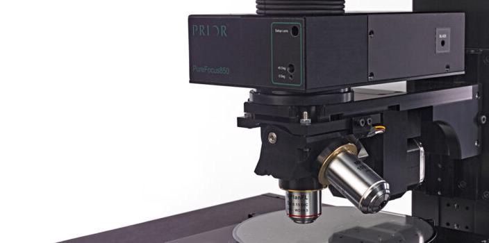
Prior Scientific released the PureFocus 850, an exceptionally versatile hardware autofocus system with the capacity to accommodate a wide range of imaging techniques, back in May 2019. Now, in 2020, multiple PureFocus 850 autofocus systems are operational in the field, improving productivity in various areas from industrial component scanning to biological research.
PureFocus 850 Autofocus: Benefits for Wafer Inspection
The PureFocus 850 is very effective for wafer inspection and has been utilized with significant success for analysis of defect selective etching. The PureFocus 850 has allowed the multinational semiconductor and electronics manufacturer, STMicroelectronics, to address and overcome several challenges related to the use of traditional autofocus systems. One of the major outcomes was reducing scanning time per sample.
STMicroelectronics use automatic image recognition software with the PureFocus 850 to analyze the quality of Silicon Carbide wafers at their manufacturing plant in Sweden. When analyzing wafer quality via defect-selective etching, it generates etch pits on the surface of the Silicon Carbide wafer. The number, morphology, and distribution of these pits signal the location and type of potential defects within a sample.
Conventional laser autofocus systems analyze signals reflected from the center of the field of view to calculate the ideal focus position. However, peripheral areas of the image may still be out of focus if the sample surface is not flat. To address this, the PureFocus 850 acquired by STMicroelectronics was calibrated to analyze signal reflected across the field of view, thus enabling consistent focus throughout every autofocus wafer scan.
Image analysis carried out while focusing on the base of the pits to analyze their morphology, meaning that the imaging plane of interest varies when compared to the main reflective surface of the Silicon Carbide wafer. This analysis is permitted by the motorized optics of the PureFocus 850, which enables offsetting of the imaging plane from the wafer surface.
STMicroelectronics also required the capability to produce both brightfield and darkfield images to facilitate their image analysis. The intuitive PureFocus 850 user interface enabled them to identify optimised settings for each imaging method based on the intensity of illumination, as opposed to having to find a compromise between the two.
PureFocus 850 Autofocus: User Benefits
Engineers using the PureFocus 850 have found it to be extremely effective autofocus system, significantly enhancing their sample analysis throughput.
I use it for all my routine inspections. Inspection times [have been] reduced from 45 minutes to 7 minutes.
Erik Sörman, Development Engineer, STMicroelectronics
The PureFocus 850 has enabled the engineers to obtain better quality images with scanning time reduce by 85% and a focus error of fewer than 10 microns.
To provide STMicroelectronics with this autofocus solution, Prior worked with BergmanLabora AB, one of Sweden’s foremost suppliers of analytical instruments. Product specialist Marie Andersson was one of the first attendees of Prior’s PureFocus 850 training sessions.
PF850 is an excellent addition to any microscope that lacks hardware autofocus. The time savings for our customers are incredibly advantageous. It has also been easy to install and maintain the PF850, as Prior’s training and support have been very good and in-depth. [The] PF850 is simply a really good product!
Marie Andersson, Product Specialist
BergmanLabora AB has since gone on to display and provide additional PureFocus 850 autofocus systems to various users in their region.
Summary
The PureFocus 850’s capabilities extend into other applications beyond Silicon Carbide autofocus wafer analysis, and increased time efficiency and optimized image quality cement the PureFocus 850 autofocus system as a system of the future. With the capacity to considerably improve throughput in a broad range of microscopic analysis processes, the PureFocus 850 is a versatile piece of image acquisition hardware that is on course to achieve popular status throughout the industry.

This information has been sourced, reviewed and adapted from materials provided by Prior Scientific Instruments Ltd.
For more information on this source, please visit Prior Scientific Instruments Ltd.