Based in France, The Institute of Electronics, Microelectronics and Nanotechnology (IEMN) is a large research center with an array of facilities dedicated to micro and nano fabrication processes.
The IEMN recently finished work on the ‘Dirac III-V’ project, which looked at approaches to producing Dirac electrons – essentially, electrons without any mass.
This high-level project necessitated the use of a wide range of fabrication and characterization techniques and a software package able to collate and process the range of different datasets generated.
Dirac III-V | Analyzing data from a large-scale multi-instrument project
Video Credit: Digital Surf
Manufacturing a Honeycomb Array in an InGaAs Quantum Well
The molecular beam epitaxy (MBE) method was used to grow a semiconductor quantum well. The challenge was to convert this quantum well into an artificial honeycomb lattice by nano-perforating an array of pores at the limit of traditional lithographic techniques.
Block copolymer lithography was employed in the production of a mask with a periodicity of 36 nm. Pores were etched into both this mask and the SiO2 protecting layer.
Scanning electron microscopy (SEM) was used following etching to accurately confirm and quantify the lattice geometry and the degree of disorder arising from the transfer of the microdomains present in the block copolymer film.
Next, the sample was transferred into a second etching machine to transfer the pores created in the mask to the InGaAs layer, effectively creating a lattice of pores in the quantum well.
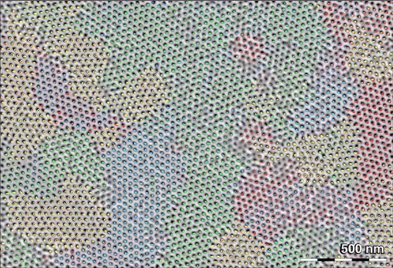
The nanoperforated quantum well imaged using SEM to check the quality of the etching processes and examine the transfer of the grain boundaries of the block copolymer mask into the SiO2 protecting layer. Image Credit: Digital Surf
Multi-physical Sample Characterization
SEM is able to produce high-resolution 2D (x,y) images, facilitating the analysis of the lateral disorder in this two-dimensional structure. Atomic force microscopy (AFM) was also employed to extract the vertical topographical information required to validate the etching processes.
The sample’s surface was oxidized and transferred back to the MBE lab for it to be cleaned and As capped, ensuring that the sample was protected against exposure to air. A combination of X-ray and UV photoelectron spectroscopy was used to characterize surface chemistry and evaluate the sample’s bond structure.
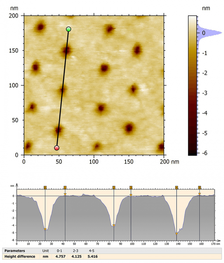
AFM was used to obtain height information on the sample and check the depth of pores. Image Credit: Digital Surf
The Nanoprobe is a multi-physical instrument housed at the IEMN. This unique device combines SEM, STM and spectroscopic techniques, enabling accurate measurement of the electrical resistivity of both the native quantum well and the nano-perforated quantum well.
The Nanoprobe instrument combines several technologies in itself: SEM, STM, optical spectroscopy etc. Image Credit: Digital Surf
On this sample we wanted to probe the conductivity of a quantum well to ensure that the sample was compatible with lower temperature measurements. All the output measurements were analyzed together in one single software; Mountains® software allowed us to correlate our results.
Maxime Berthe, SPM Development Engineer.
Scanning tunneling microscopy (STM) – a surface-sensitive technique – was also used to acquire accurate morphology information and to investigate the outstanding electronic properties of the nano-perforated quantum well.
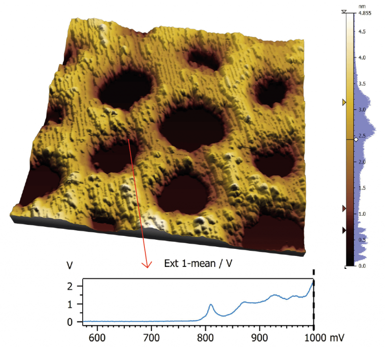
Scanning tunneling spectroscopy (STS) data processing was performed using Mountains®. Image Credit: Digital Surf
Once the measurements were completed and the data acquired, the next step was to extract some useful information and that’s where Mountains® software is very useful because we can process both topography and spectroscopy data in the same place.
Nemanja Peric, PhD Researcher, IEMN.
Project Results
The project was very challenging but rewarding when we were able to show the existence of specific electron states and finally the state we are looking for.
Mountains® was key to processing the different nanofabrication steps involving multi-physical analysis and finally to prove the existence of electrons with very light mass.
Bruno Grandidier, Project Leader
References
- Engineering a Robust Flat Band in III–V Semiconductor Heterostructures, N. Franchina Vergel et al., Nano Lett. 2021, 21, 1, 680–685, Dec. 2020. doi.org/10.1021/acs.nanolett.0c04268

This information has been sourced, reviewed and adapted from materials provided by Digital Surf.
For more information on this source, please visit Digital Surf.