The main obstacle to the wider adoption of graphene in electronics and optoelectronics is the material's lack of an intrinsic electronic bandgap, making the production of graphene-based field-effect transistors and other electronic devices difficult. Researchers from Stanford University and Shanghai Jiao Tong University recently created one-dimensional graphene nanoribbons (GNRs) that are less than 10 nm by squashing carbon nanotubes using a thermally assisted high-pressure process. Such GNRs behave like semiconductors and can meet the application requirements of high-performance logic devices.
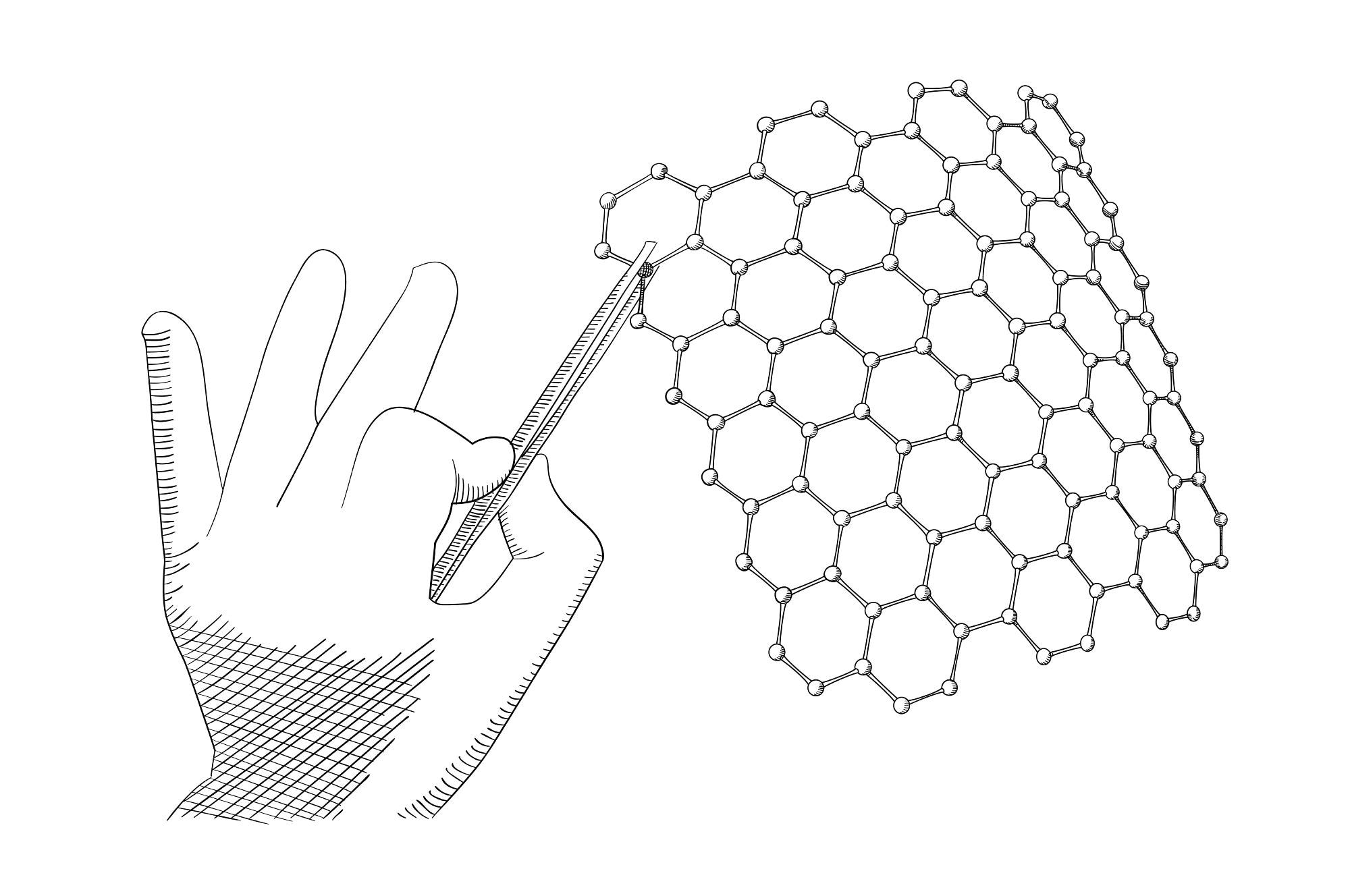
Image Credit: Perception7/Shutterstock.com
Graphene, a carbon allotrope consisting of a monoatomic layer of carbon atoms organized in a hexagonal lattice, exhibits superior mechanical strength, high thermal conductivity, strong light-matter interactions, and, in particular, exceptional electronic properties.
These properties make graphene an outstanding material for numerous potential applications in energy storage, electronics, and material science. However, creating graphene-based high-performance transistors, one of the most appealing applications of graphene with huge market potential, is still in the future. The fundamental problem that hinders the application of graphene in electronics is the absence of an intrinsic electronic bandgap in the material.
A Limit to the Miniaturization of Silicon-Based Transistors
Currently, reducing the size of the traditional silicon-based transistors ensures constant performance improvement in microelectronics. Despite this, the existing technology is close to the limit of how small these devices can be made. Hence, microelectronics manufacturers are turning their attention to graphene for the next generation of high-performance devices.
Semiconductors are characterized by their bandgap, which is the energy required to excite an electron from the valence band, where it cannot conduct electricity, to the conduction band of the semiconducting material. This bandgap needs to be large enough to guarantee a distinct contrast between the on and off states of the transistor, enabling information processing without errors.
Zero Bandgap and Outstanding Electrical Properties
Unlike silicon-based semiconductors, pristine two-dimensional sheets of graphene behave as a semimetal with a zero bandgap. This contributes to the material's exceptionally high electron mobility at room temperature, also known as ballistic transport, and outstanding thermal conductivity. However, previous studies have demonstrated that a distinct bandgap can be induced by confining graphene's dimensions into narrow ribbons with a width of a few nanometers, thus producing semiconductive GNRs.
The bandgap in GNRs originates mainly from quantum confinement of the electronic states in the material as one of the dimensions is reduced, allowing to tune the electronic properties of GNRs as a function of their width and edge structure.
Bandgap Opens in Graphene Nanoribbons
Earlier attempts to create GNRs included opening up single-walled carbon nanotubes (SWCNTs) or lithographically patterning GNRs from two-dimensional graphene sheets. These methods yielded GNRs with rough edges that degraded their electronic properties.
More recent experiments have demonstrated that bottom-up chemical synthesis routes (assembling GNRs on substrates from molecular precursors) resulted in an ultra-narrow (less than 2 nm wide) GNRs with uniform width and atomically-precise edges. Such high structural homogeneity showed a great promise for the integration of GNR in field-effect transistors (FETs). However, the complexity of the bottom-up synthesis has so far prevented the large-scale adoption of GNRs in high-performance FETs.
Squashing Carbon Nanotubes into Nanoribbons
Recently, an international research team from the USA and China led by Hongjie Dai, a professor of chemistry at Stanford University, has demonstrated that long, narrow GNRs with atomically-smooth edges can be created by treating SWCNTs with high pressure and high temperature. Single-walled carbon nanotubes essentially represent a sheet of graphene rolled into a cylinder. Collapsing such a structure can yield a double stack of long GNRs with atomically smooth closed edges.
Structural collapse of large-diameter carbon nanotubes has been observed previously. However, the approach developed by the Chinese-American team yields GNRs as narrow as 1.4 nm, a value smaller than the theoretically predicted minimum width of 2.6 nm for SWCNTs to remain in stable flattened conformation.
To achieve this, Prof. Dai and his collaborators used a high-pressure diamond anvil cell where a batch of SWCNTs was compressed between two diamond anvils. To stabilize the collapsed structure, the sample was heated to 220°C for 40 min followed by rapid cooling to room temperature. The combination of high pressure and high-temperature annealing led to irreversible deformation of the closed edges of the GNRs.
GNRs with Enormous Potential for Electronic Applications
As a proof-of-concept, the researchers fabricated a FET device containing a 2.8 nm-wide GNR that exhibited an on/off current ratio of more than 104, charge mobility of 2443 cm2 V–1 s–1, and a bandgap of 0.5 eV (almost double of that of earlier GNR-based FETs). Experimental results suggested that these high-quality, long and narrow, semiconducting GNRs are well suited for potential use in microelectronics.
Prof. Dai's team hopes that further development of the method would make feasible the large-scale production of narrower GNRs with atomically-smooth edges that eventually could replace silicon in the next-generation transistors. Notably, the technique can be extended to make nanoribbons from other materials by collapsing metallic nanotubes.
Continue reading: Synthesis Techniques of Graphene Oxide: An Overview.
References and Further Reading
I. Fadelli (2021) A technique to create sub-10-nm graphene nanoribbons from squashed carbon nanotubes [Online] www.phys.org Available at: https://phys.org/news/2021-09-technique-sub-nm-graphene-nanoribbons-carbon.html
R. Peleg (2021) New method creates sub-10-nm GNRs from squashed carbon nanotubes [Online] www.graphene-info.com Available at: https://www.graphene-info.com/new-method-creates-sub-10-nm-gnrs-squashed-carbon-nanotubes (Accessed on 28 October 2021).
Chen, C., et al. (2021) Sub-10-nm graphene nanoribbons with atomically smooth edges from squashed carbon nanotubes. Nat. Electron. 4, 653–663. Available at: https://doi.org/10.1038/s41928-021-00633-6
Toh, C.T. (2021) Squashing carbon nanotubes into nanoribbons. Nat. Electron. 4, 633–634. Available at: https://doi.org/10.1038/s41928-021-00645-2
Koen Houtsma, R.S., et al. (2021) Atomically precise graphene nanoribbons: interplay of structural and electronic properties. Chem. Soc. Rev., 50, 6541-6568. Available at: https://doi.org/10.1039/D0CS01541E
Disclaimer: The views expressed here are those of the author expressed in their private capacity and do not necessarily represent the views of AZoM.com Limited T/A AZoNetwork the owner and operator of this website. This disclaimer forms part of the Terms and conditions of use of this website.