Over the last 20 years, the proliferation of research utilizing scanning electron microscopy (SEM) has driven the performance of systems towards higher resolution at lower voltages.
This enthusiasm is driven by the need to understand surface structures and their chemistry, thanks to breakthroughs in such fields as metamaterials, 2D materials and semiconductor device manufacturing approaching the limit of Moore’s law.
Electron optical columns are essential to the functioning of any SEM, conventional or field emission SEM (FE-SEM). Based upon the Gemini column design, the ZEISS FE-SEMs have undergone a plethora of technological advancements since its launch in 1993.
Low acceleration voltage imaging is appealing because it decreases the interaction volume in the specimen, allowing surface-sensitive information to be obtained.
In addition, the charging of insulating samples by SEM investigation can be evaded by decreasing the electron energy used to probe the sample. The lowered radiation damage from low-energy SEM imaging is also critical for imaging sensitive specimens such as semiconductor devices and biological samples.1
Advancements in Objective Lens Designs
It is well understood that specially designed lenses with low spherical and chromatic aberration (Cs and Cc) are required to obtain a fine electron probe size at low energy.
Basic implementations can be made to overcome this problem, such as immersing the specimen in either a strong electric field (sample bias) or a strong magnetic field (magnetic single-pole lens), or even both.
However, these methodologies impose severe restrictions on the sample types that can be analyzed, besides their shape and the ability to tilt such samples.
By using the Gemini design – the combination of in-column beam deceleration and an enclosed magnetic lens – it is possible to achieve comparable, if not higher, resolution than immersion-type lenses.
This can be achieved while also avoiding the immersion of the sample in an electromagnetic field and maintaining a high degree of sample flexibility.2
In 1993, ZEISS developed the first commercial FE-SEM, the DSM-982, with Gemini electron optics based on such a principle.
Distinctive properties of this compound lens include decreasing spherical and chromatic aberrations (Cs and Cc) with electron energy (Fig. 1). This helps achieve a high resolution at very low beam energies, such as those lower than 1 keV.
The DSM-982 was the first commercial SEM to exhibit resolution greater than 10 nm with less than 1 keV electron energy.3 Based on the same concept as a compound magnetic-electrostatic lens, the Gemini electron optics were continually improved over the following decades.
In 2015, equipped with the Nanotwin lens, the ZEISS GeminiSEM 500 was launched. Its Cc and Cs values decreased to less than one-third of the original Gemini lens design.
In addition, this design further diminished the magnetic field strength on the sample, which was already a factor of 1000 less than the sample experiences with an immersion lens.
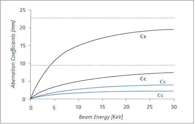
Figure 1. Spherical and chromatic aberrations (Cs and Cs) of the original Gemini lens (black curve) and the Nano-twin lens (blue curve) with respect to different beam energies at 1 mm working distance. Image Credit: Carl Zeiss Microscopy GmbH
Smart Autopilot Electron Optical Engine
ZEISS has introduced several technical achievements, expanding the performance and usability of the Gemini column design by an improved Nano-twin lens. Furthermore, these developments result in a resolution less than 1 nm below 1 kV without immersing the specimen in a magnetic or electrical field.
Owing to a novel electron-optical (EO) engine, the Smart Autopilot, the beam convergence angle is enhanced on the fly for the current working condition, enabling the best possible resolution.
The new engine includes a new scanning mode, providing a seamless transition between sample navigation over large distances, high-resolution imaging and a very large field of view. Lastly, the Smart Autopilot provides beam alignment using a patented parallax method and an extremely rapid automated focus.
Examples of high-resolution images acquired at low beam energy are displayed in the following figures.
The montmorillonite particles depicted in Fig. 2 are non-conducting. This specimen is imaged at 800 V using a 15 pA current by choosing a corresponding aperture size, thus avoiding charging.
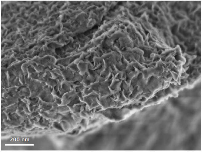
Figure 2. High resolution image of montmorillonite particles obtained at 800 V beam energy. Even though the sample is non-conductive, fine flakes on the fractured surface can be well resolved. Image Credit: Carl Zeiss Microscopy GmbH
The Smart Autopilot automatically enhances the condenser excitation to produce the best possible resolution for this specific condition. As such a sample is not conductive, it is not reasonable to apply a potential on the specimen. This would result in electrostatic charging effects, which could potentially damage the system.
Luckily, such potential is not essential to produce an image of exceptional resolution with the Gemini column design in combination with a Nano-twin lens and Smart Autopilot.
Likewise, the FeMn magnetic nanoparticles shown in Fig. 3 cannot be immersed in a magnetic field for imaging. This would result in nanoparticles being attracted towards the lens, causing potential damage to the SEM’s optical system.
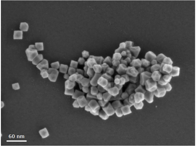
Figure 3. High resolution image of FeMn magnetic nanoparticles obtained at 1 kV beam energy. Even though the sample is magnetic, the highest resolution can still be achieved. Image Credit: Carl Zeiss Microscopy GmbH
Again, utilizing the Gemini column design with Nano-twin lens and Smart Autopilot, this problem is overcome by the known Gemini optical design principle.
While the resolution is often used as the benchmark of any SEM, the significance of lower magnification performance is frequently underappreciated. The new Smart Autopilot engine from ZEISS provides a novel scanning mode, allowing a large field of view (FoV) that aids navigation across the specimen.
This is accomplished by using a different arrangement of the scanning system while continuing to maintain the lens configuration and beam energy unaltered.
This guarantees a quick transition between the large field of view mode and normal imaging mode without altering the voltage of any electron-optic components, and all detectors in the FE-SEM system maintain a consistent contrast and performance.
In the Fig. 4 example, three Euro coins are imaged at 5 kV beam energy. In normal imaging mode, the maximum FoV is approximately 4 mm – only enough to cover a small portion of a single coin. The Smart Autopilot engine drives the system, allowing all three coins to be imaged within the same frame.
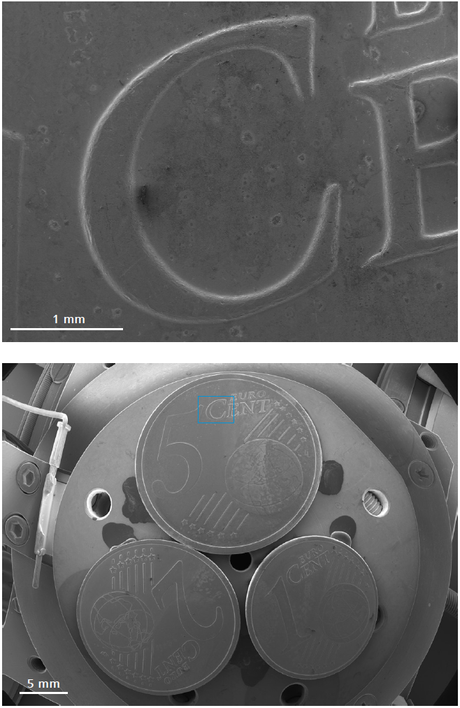
Figure 4. Euro coins imaged at maximum FoV in normal imaging mode (upper) and in high FoV mode (lower) using the new EO engine Smart Autopilot. The blue square shows the position and size of maximum FoV in normal imaging mode. Image Credit: Carl Zeiss Microscopy GmbH
An additional advantage of the Smart Autopilot engine is illustrated in the resulting auto-functions for beam alignment and fine focusing. EO calculations are used to align the microscope and adjust the focus.
The time to results is detailed in Table 1, evidencing the fast autofocusing time.
Table 1. Performance of EO engine-based auto-functions. Source: Carl Zeiss Microscopy GmbH
| |
Duration |
| Autofocus |
<1 s |
| Auto align |
<4 s |
For example, in Fig. 5, the precision of the fine autofocus is presented in an image pair before and after autofocusing. These new capabilities complement the auto-stigmation, auto-contrast brightness and coarse-autofocus functions that are available.
As a result of its varying degrees of automation, ease of use and superior speed, this technology will be available to all users, independent of their skills.
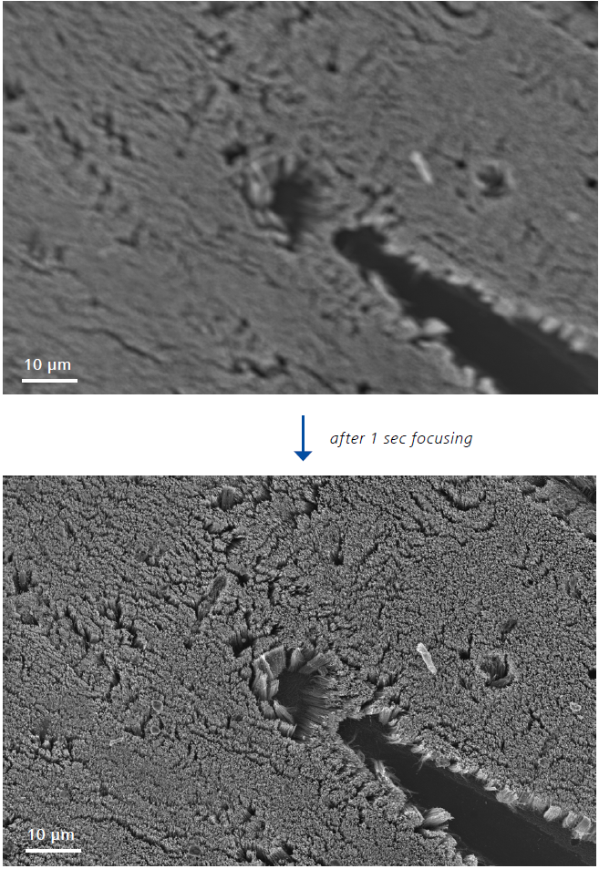
Figure 5. Example of ultra-fast fine focus. Sample: carbon nanotube forrest. Image Credit: Carl Zeiss Microscopy GmbH
Conclusion
After developing the pioneering low kV imaging without using immersion lenses, ZEISS has continually pushed innovation in this field, introducing the Nano-twin lens in 2015 and with their latest development, the new engine Smart Autopilot.
Smart Autopilot further improves resolution at low kV by optimizing the convergence angle of electrons traveling through the column at given conditions. In addition, the Smart Autopilot significantly enlarges the available field of view by using the high-performance Nano-twin lens.
This system's ease of use is enhanced further through the Smart Autopilot’s new auto beam alignment and autofocus functions. In particular, the system's new autofocus capabilities bring the operation into the millisecond domain for the first time.
Acknowledgments
Produced using material originally authored by Dr. Luyang Han and Dr. Benjamin Tordoff, from Carl Zeiss Microscopy.
References
- Reimer, L. Imaging formation in low-voltage scanning electron microcopy. SPIE optical engineering press, 1993.
- Orloff, J. Handbook of Charged Particle Optics (2nd edition). CRC Press, 2009.
- Jaksch, H. & Martin, J. P. High-resolution, low-voltage SEM for true surface imaging and analysis. Journal of Analytical Chemistry, Volume 353, Issue 3-4, pp 378-382, October 1995.

This information has been sourced, reviewed and adapted from materials provided by Carl Zeiss Microscopy GmbH.
For more information on this source, please visit Carl Zeiss Microscopy GmbH.