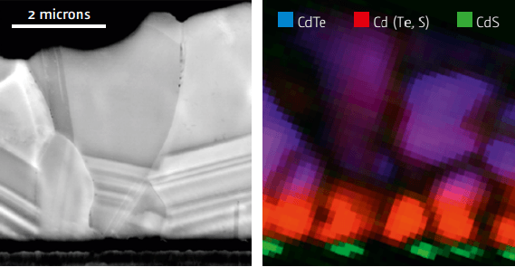
Figure 1. SEM and Quantitative CL map of Photovoltaic Heterojunction
(a) SEM image of cross-section of CdTe/CdS photovoltaic heterojunction
(b) CL map of the same cross section color-coded by emission frequency. Note the diffusion of sulfur at the junction
Capture the Power of Light Within
Electron microscopists have long had a matrix of e-beam and x-ray spectroscopies in their arsenal. However, cathodoluminescence (spectroscopic analysis of electron-activated light) has presented a unique set of challenges in terms of alignment, limited field of view, uniformity, and reproducibility.
New, fully integrated CL-SEM systems from Attolight solve those problems, requiring zero instrument alignment, producing 300mm fields of view without stitching, at very high speeds, with true quantitative results.
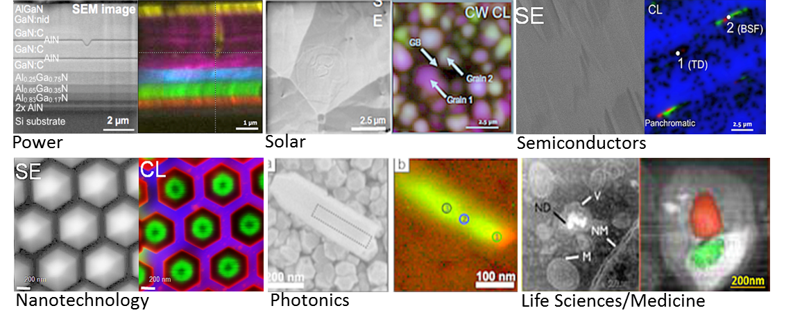
Figure 2. CL-SEM can be used across many different disciplines;
Power- HEMT stack cross section
Solar – CdTe PhotoVoltaic grain boundary study
Semiconductors – Threading dislocation and Basal Stacking Fault in epilayer of GaN
Photonics – InGaN nanowires
Nanotech - Strain analysis, GaN/AlGaN core-shell structure
Life Sciences/Medicine - Vesicle classification using functionalized nanodiamonds (V=vesicle, NM = Nuclear membrane, M = mitochondria; L = SE image; R = HAADF w/CL overlay
Attolight’s Next-Generation Integrated Optical/Electron Column Design
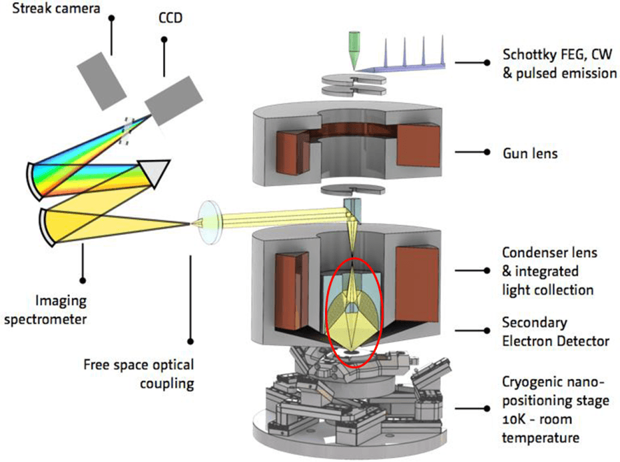
Figure 3. Attolight's integrated optical/electron column design eliminates instrument alignment and increases speed to produce uniform, reproducible electron imaging and hyperspectral CL analysis over very large fields of view (300mm). The result: fast time-to-results.
Benefits:
Designed from the ground up as an integrated CL-SEM system (Figure 2, red circle) puts optical collection within the electron column
- Requires ZERO instrument alignment
- Ensures CL uniformity and reproducibility, making the system quantitative as well as qualitative
- Uses lower beam dosages, reducing the possibility for beam damage to sensitive samples
- Fast! Measurement time range from 5s -30min compared to the competition’s 30min –multiple hours
High numerical aperture optical objective (NA=0.71)
- Enables much larger field of view (300mm) compared to parabolic mirror systems
- 0% photon loss due to vignetting in polychromatic mode
- Comfortable 3mm working distance
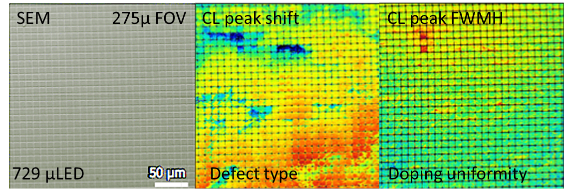
Figure 4. SEM and Quantitative CL map of microLEDs (300mm field of view, unstitched)
(a) Secondary electron SEM image
(b) CL image showing InGaN peak shift illustrating defect type
(c) CL Image showing same peak shift, illustrating doping uniformity (Sample: Array of 8x8µ microLEDs separated by 1µ spaces)
High current densities; low voltage
- 30nA for spots <10nm; 250nA for spot size <25nm
- 3-10kV for optimum contrast
Conventional or high speed hyperspectral imaging
- 2D RGB hyperspectral maps; 3D maps
- Ability to spectrally slice the hypercube for specific wavelengths to isolate/identify local phenomenon and structures
Intuitive User Interface and specialized software
- Touch screen based
- Context-based
- Attomap™ hyperspectral analysis software
Integrated cryogenic Nano-positioning stage (optional: 10K to room temperature)
- Assures low drift
- Minimal vibration
Unique scanning modes for full wafer characterization without cutting wafer (up to 300mm)
Continuous Upgrade Path
- Time resolved CL with on-the-fly changeover from continuous to pulsed mode (<10 psec decay times)
- Cryo stage for ultra-low thermal drift
- EBIC, EBAC, RCI (fully compatible with cryo stage)
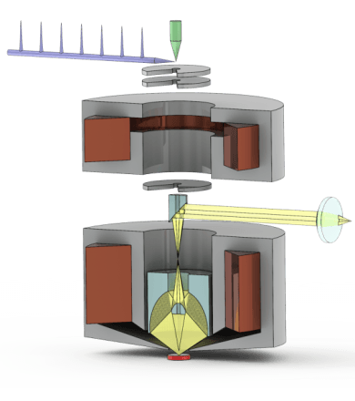
Figure 5. As with all our advanced techniques, Attolight's unique pulsed-mode option for time resolved CL can readily be added to our more basic systems.
| Instrument |
Hyperspectral CL Mapping |
Thermal Range |
Spectral Range |
Time Resolved |
| Grammont 2172 |
Conventional |
Room Temp |
UV-NIR |
No |
| Allalin 402 |
Ultrahigh speed |
Cryo |
UV-NIR |
No |
| Rosa 4634 |
Ultrahigh speed |
Cryo |
UV - Full IR |
No |
| Allalin 4027 Chronos |
Ultrahigh speed |
Cryo |
UV - Vis |
pSec TS |