Mar 6 2009
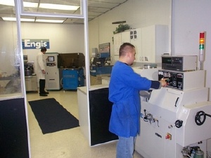
Leading developer of diamond superabrasive finishing systems for the manufacture of MEMS, data storage components, optics and opto-electronics, Engis Corporation has created a network of Advanced Materials Processing Laboratories around the world, first at its Illinois HQ, and now in Japan and the UK, where the Henley-on-Thames facility provides a European resource for developers seeking technical support and expertise in polishing and thinning of advanced materials.

In these laboratories expert staff work directly with manufacturers and researchers to solve the technical challenges posed by processing the raft of new materials now being used in the production environment. This close collaboration enables new production processes to be developed concurrently with product designs, so delivering highly technical products to the market more quickly and with greater reliability.
The core concept behind the Advanced Materials Laboratories is Engis' integrated approach to diamond superabrasive technology, which brings together all the different components of the process, from machine tools, plates, pads and facing tools equipment to consumables such as slurries and lubricants, into one unified solution, each element of which is under Engis' complete control. Staff in the network of laboratories work together, pooling their expertise to focus on an individual polishing and lapping requirement, providing global expertise at a local level.
The first stage in the development process is to obtain an in-depth understanding of the requirements of each customer, creating a modular process to suit each unique set of requirements, including constraints such as existing equipment, waste management and disposal legislation and/or requirements, speed of throughput and operational cost demands.
Having completely understood the requirements and constraints of the process the unique chemical and mechanical properties of the materials are considered, so that the optimum slurry can be selected, or, if necessary, developed specifically to suit the application, using precisely graded micron diamond which can process extremely hard and chemical resisting materials such as Sapphire, Silicon Carbide, III - V Nitrides and other substrate materials which are frequently used for MEMS and nanotechnology applications.
This level of bespoke development is only possible due to Engis own R&D laboratories and production facilities which enable process engineers to control all the variables including exactly how the diamond is micronized and how the slurry is formulated, the selection and correct charging of the appropriate composite lapping plate and how each production cycle is set up and run.
When all the variables have been examined the whole process is examined in detail once again in order to improve the performance of less expensive earlier steps, to save time and money during more expensive later steps and so create the optimum system of individual process modules, including mounting, machines, slurries and plates, texturing and cleaning.
This laboratory-based solution development provides end-product manufacturers and researchers with real benefits in terms of shorter cycle times, reduced overall consumables costs and shortened CMP process step due to better semi-finishing processes.
It also enables customers to move to "greener", more eco-friendly production processes through a reduced level of consumables and slurry consumption and hence waste disposal and the use of water-soluble easily-cleaned diamond slurries and non-freezing CMP slurries which are less prone to crystallization, while, at the same time maintaining and even enhancing production levels.
Engis MD, John Wellings comments, "Materials such as Gallium Nitride and Silicon Carbide pose specific challenges to developers. Because Engis undertakes extensive R&D activities in its own right, as well as working closely with academic institutions on a range of funded projects, we understand those challenges and are able to assist with leading edge technical expertise."