Nov 3 2009
Leaders of the chip making industry at this year's ISMI Symposium on Manufacturing Effectiveness examined how engineers used a wireless method to measure the gap between a plasma-enhanced chemical vapor deposition (PECVD) heater and showerhead and improved first pass film checks by 24 percent during a session on equipment productivity with the CTO of CyberOptics Semiconductor, Craig C. Ramsey, Ph.D.
 Engineers increased the first pass film-check rate from 80 percent to over 99 percent, as well as chamber availability by four percent using a wireless gap-measurement method that employs the WaferSense(R) Auto Gapping System (AGS).
At the 6th annual symposium, which offered attendees information to reduce manufacturing expenses and increase productivity, Ramsey addressed how engineers control gap uniformity and magnitude with high stability over time. He contrasted a legacy gap-measurement method used by engineers that employs a wired leveling device and crush blocks with a method that employs a wireless gapping device and NIST traceable gap field standard.
Ramsey detailed how the legacy method led to lower first pass film checks -- with 20 percent of chambers failing film checks -- and lower chamber availability, as well as increased maintenance cycle time and expenses. Ramsey added that the legacy method isn't a repeatable process and doesn't yield reproducible data. Measurements obtained by the wired leveling device and crush blocks are susceptible to instrument and operator variances.
Engineers often repeat the legacy gapping process multiple times before a chamber comes within the gap tolerances required to deposit quality films, according to Ramsey. The films are then deposited onto monitor wafers and the average thickness and thickness uniformity are measured to ensure that films are within specification.
"And when films fail the parametric check with the legacy method, the gapping process must be repeated and six hours of chamber production time is lost," Ramsey said. "When you walk through the steps of the legacy gapping method, you really see the extra work and challenges the instruments present."
Ramsey's presentation, titled "Improved Film Production in a High-Volume Fab," detailed how engineers increased the first pass film-check rate from 80 percent to over 99 percent, as well as chamber availability by four percent using the wireless gap-measurement method. The wireless method is repeatable and gives engineers data to optimize their preventive maintenance (PM) schedules and process controls, according to Ramsey.
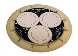
The wireless device used by engineers contains three non-contact distance sensors that return gap measurements in real time to a laptop or PC in numerical and graphical form. Engineers used the device to ensure gaps were accurate and uniform to allow for enough film at the proper thickness. The vacuum-compatible device also minimized the possibility of chamber contamination and shortened the total tool maintenance cycle.
"Average film-thickness variation was maintained within specification with the wireless gap-measurement method," Ramsey said. "And the fab experienced improved film production."
Ramsey said the wireless gap-measurement device is the WaferSense® Auto Gapping System (AGS).
The AGS' parallelism accuracy is 0.025 mm (+/-0.001"), and its gap accuracy is 0.025 mm (+/-0.001") with a gap of 15 mm (0.600"). The AGS is available in 200 and 300 mm form factors, with the AGS300 being the best-known method (BKM) -- for 40 percent improvement in film uniformity -- for gapping Novellus VECTOR® tool chambers.
CyberOptics Semiconductor is a maker of wireless metrology devices for wafer processing equipment. The company's WaferSense family of devices includes the Airborne Particle Sensor (APS), Auto Leveling System (ALS2 Vertical), Auto Vibration System (AVS) and Auto Teaching System (ATS). Each device follows the processing life of a wafer and reports real-time metrology data.