Sep 15 2009
Novelx, Inc. was just selected as the runner-up for a Wall Street Journal Technology Innovation Award in the Materials and Other Base Technologies category. The Wall Street Journal recognized Novelx for using silicon processing technologies to miniaturize the core technology inside a scanning electron microscope (SEM).
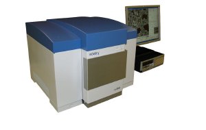
Powered by the patented Novelx Stacked Silicon Technology, the Novelx mySEM is a bench-top SEM for imaging and characterizing nanoscale objects and materials. In a compact design that installs easily into available lab space or closer to production lines, the mySEM delivers capabilities previously only available in high-end field emission SEMs, at a fraction of the cost. Optimized for low-voltage operation and without the need to coat non-conductive samples, the mySEM is an ideal choice for the imaging of energy sensitive nanomaterials, biomaterials, polymers, thin films and membranes.
Lawrence Muray, CEO and co-founder of Novelx, explains, “Novelx is the only company building SEMs wafer scale using semiconductor processing technologies. By doing so, Novelx has decreased the size of the core technology in a SEM by orders of magnitude and reduced the cost by over half while delivering best-in-class imaging capabilities previously only available in highend SEMs."
For this year’s Wall Street Journal Technology Innovation Awards, judges considered whether innovations were truly groundbreaking and whether their application would be particularly useful in a time of economic hardship. According to John Leger, News Editor at the Wall Street Journal, “It was an extremely competitive contest this year with nearly 500 entries from 20 different countries." The Wall Street Journal editorial staff and an independent panel of expert judges were looking for innovations that broke with conventional processes and went beyond marginal improvements in existing products and services to have a wide impact.
Jim Rynne, VP of Business Development at Novelx, describes the market opportunity, “The mySEM will make nanoscale imaging more accessible by distributing high-resolution and lowvoltage imaging capabilities more broadly and cost-effectively. The market timing for such a solution is ideal as the size of silicon features continues to shrink according to Moore’s law and the number of new product innovations incorporating nanomaterials increases. The imaging capabilities of the mySEM are needed to both speed new product development cycles and to move nanoscale quality assurance closer to production lines"
The Novelx mySEM is commercially available and in use by several leading university research centers for the imaging of nanoscale objects and materials in a wide variety of fields that include materials science and the life sciences. Industrial applications include the characterization of nanomaterials at corporate product development labs, the failure analysis of nanoscale defects and the quality assurance of products designed with nanomaterials.
For additional information on the news that is the subject of this release, contact Jim Rynne or visit www.novelx.com.