Jan 21 2013
The National Institute of Advanced Industrial Science and Technology and the National Institute for Materials Science jointly developed a graphene transistor based on a new operating principle.
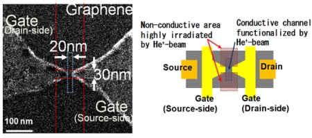 Figure: Helium ion microscope image and schematic diagram of the prototype device.
A team headed by Dr. Naoki Yokoyama, Leader of the Collaborative Research Team Green Nanoelectronics Center (hereinafter, GNC) of the Nanoelectronics Research Institute (Director: Seigo Kanemaru) at the National Institute of Advanced Industrial Science and Technology (hereinafter, AIST; President: Tamotsu Nomakuchi), Dr. Shu Nakaharai, a Designated Intensive Researcher, also of the GNC, and Dr. Shinichi Ogawa, an Invited Researcher at the Nanoelectronics Research Institute, in joint research with the AIST Innovation Center for Advanced Nanodevices (Director: Hiroyuki Akinaga) and a team headed by Dr. Kazuhito Tsukagoshi, a MANA Principal Investigator at the International Center for Materials Nanoarchitectonics (hereinafter, WPI-MANA; Director-General: Masakazu Aono) of the National Institute for Materials Science (hereinafter, NIMS; President: Sukekatsu Ushioda), developed a graphene transistor based on a new operating principle.
In the newly-developed transistor, two electrodes and two top gates were arranged on the graphene, and crystal defects were introduced by irradiating a helium ion beam on the graphene between the top gates. Charge movement can be controlled efficiently by applying an independent voltage to the two top gates. The device displayed a current ON/OFF ratio of approximately 4 orders at 200K (-73°C).
In addition, transistor polarity can be reversed by electrical control. No transistor has been capable of this type of operation until now.
This technology can be used in existing manufacturing technology for silicon integrated circuits. It is expected to contribute to realization of ultra-low power consumption electronics by reduction of the operating voltage in the future.
Details of this technology will be announced at the international conference 2012 International Electron Devices Meeting (IEDM 2012), held in San Francisco (United States) December 10-12, 2012.
*This research is granted by the Japan Society for the Promotion of Science (JSPS) through the Funding Program for World-Leading Innovative R&D on Science and Technology (FIRST Program)",initiated by the Council for Science and Technology Policy (CSTP).