Dec 11 2013
Xilinx, Inc. today announced a new record breaking 4.4M logic cell device, more than doubling its industry leading highest capacity Virtex®-7 2000T device, achieving two consecutive generations of high-end leadership, and delivering an extra node worth of customer value.
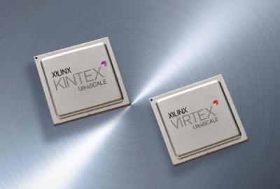
 Xilinx 20nm All Programmable UltraScale Portfolio delivers an ASIC-class advantage with the industry's only ASIC-class programmable architecture coupled with the Vivado ASIC-strength design suite and UltraFast design methodology. (PRNewsFoto/Xilinx, Inc.) source: XILINX, INC.
As the highest end device of Xilinx's All Programmable UltraScale™ portfolio, also announced today, the Virtex® UltraScale™ VU440 3D IC extends Xilinx's industry lead from 2x at 28nm to 4x at 20nm – offering greater capacity than any other programmable device. Using advanced 3D IC technology, the VU440 device delivers more at 20nm than publicly stated competitive plans at 14/16nm.
The Virtex UltraScale VU440 device sets a new industry benchmark, delivering 50M equivalent ASIC gates for next generation production and prototyping applications. 20nm Virtex UltraScale devices also provide the highest system performance and bandwidth for single chip implementations of 400G MuxSAR, 400G Transponder and 400G MAC-to Interlaken bridge applications.
"Synopsys has used six generations of Xilinx devices for our fully integrated hardware and software HAPS® FPGA-based prototyping systems," said John Koeter, vice president of marketing for IP and systems at Synopsys. "We anticipate the combination of the Xilinx Virtex UltraScale VU440 functionality combined with HAPS' unique system capabilities will increase overall system performance and capacity resulting in higher productivity for early software development, hardware/software integration and SoC system validation."
The Virtex UltraScale family gives customers new levels of performance, systems integration, and bandwidth with the added benefits of re-programmability. The scalability of the Virtex UltraScale VU440 device is made possible by its ASIC-class architecture – for up to 90% utilization featuring next generation routing, ASIC-like clocking, power management, elimination of interconnect bottlenecks, and critical path optimizations. Along with major advancements to key architectural blocks—such as wider multipliers, high speed memory cascading, 33G capable transceivers, and the addition of industry leading integrated 100Gb/s Ethernet MAC and 150Gb/s Interlaken IP cores, these devices enable multi-hundred gigabit-per-second levels of system performance with smart processing at full line rates.
"ARM has used previous generations of Virtex FPGAs for our IP validation. The UltraScale Architectural innovations, combined with Vivado, enable higher utilization and performance than has been achieved previously," said Spencer Saunders, director of hardware acceleration at ARM®. "The tremendous gate capacity, excellent serial bandwidth and impressive input/output pin count offered by Virtex UltraScale is ideal for enabling the next generation of IP development."
Key to the device's industry leading bandwidth and capacity is second generation Stacked Silicon Interconnect (SSI) technology. Built on TSMC's CoWoS manufacturing technology, this generation of SSI technology features 5x more inter-die bandwidth and a unified clocking architecture across slice boundaries to deliver a virtual monolithic design experience. Xilinx's SSI technology enables Xilinx to deliver devices with 2-4x the capacity of competing devices and continue to stay ahead of what Moore's Law could otherwise offer. Xilinx first debuted its SSI technology with its Virtex-7 2000T device in 2011 – the world's highest capacity device at that time – built with 6.8 billion transistors, providing customers access to an unprecedented 2M logic cells, equivalent to 20M ASIC gates.
Xilinx UltraScale devices deliver an ASIC-class advantage with the industry's only ASIC-class programmable architecture that scales from 20nm planar through 16nm FinFET technologies and from monolithic through 3D ICs. Through a combination of TSMC's leading-edge technology and co-optimization with the Vivado ASIC-strength Design Suite, and recently introduced UltraFast™ design methodology, Xilinx is one to two years ahead in delivering another 1.5x to 2x realizable system-level performance and integration.
Source: http://www.xilinx.com/