QuantumWise has released a new version of their software platform for atomic-scale modeling, Virtual NanoLab, and the simulation engine Atomistix ToolKit. The focus of this release is applications to semiconductor problems.
Over the past 24 months, QuantumWise has acquired several new customers within the semiconductor industry who are looking to the company for solutions on atomic-scale modeling.
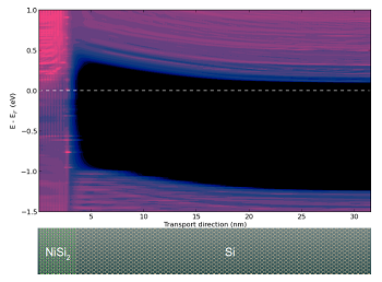 First-principles simulations of a metal-semiconductor (NiSi2/Si) interface with an accurate band gap for the doped semiconductor side, showing a Schottky barrier formation at the interface.
The need for a detailed understanding of new materials and novel device structures is growing rapidly as the traditional models provided by TCAD (Technology Computer Aided Design) are starting to fail, due to the fact that they don’t encapsulate the detailed physics on the nanoscale.
“Many of the new features in the 2014 version are developed in direct response to urgent requests from our key customers in the semiconductor industry”, says Anders Blom, Chief Customer Officer at QuantumWise. “We have focused on developing solutions that enable them to use atomic-scale modeling in their research and development of nanoscale devices as efficiently as possible. This involves both particular features and guidance in the form of new public tutorials and consultancy work performed with individual customers.”
New features in the 2014 release
The new features involve spin-orbit interaction and Meta-GGA for accurate first-principles prediction of band structures of both bulk semiconductor materials and confined structures like nanowires. For such systems it is important to consider surface passivation and doping, and new methods have been added for this. Moreover, the inclusion of noncollinear spin enables the computation of spin transfer torque and other properties of magnetic tunnel junctions, a possible replacement of memory cells in the future. The new version of ATK is up to 35% faster for density functional theory (DFT) and tight-binding calculations.
ATK 2014 also expands the types of problems that can be studied with the software by making it possible to compute mechanical and thermal properties, in addition to the electronic transport properties that have been the hallmark of ATK for over 10 years. These new features have been developed in collaboration with the Fraunhofer SCAI institute in Bonn, Germany, in a project funded by the European Union under the Eurostars program. In this project, ATK has been expanded with a new module called ATK-Classical, with the capability to use empirical potentials to perform e.g. molecular dynamics simulations.
With a particular focus on semiconductor problems, new tools have also been designed to use these classical potentials to study elastic properties, thermal transport across grain boundaries, creep strain in polycrystalline structures, and other properties that are relevant for materials for modern semiconductor materials. This list will be further expanded during the remaining 6 months of the project, to consider e.g. ion implantation and crystal growth simulations, as well as dopant diffusion.
From interface to platform
Another major new development in the 2014 release is that Virtual NanoLab has been expanded to act as a graphical user interface for other codes, like VASP, Quantum Espresso, LAMMPS, etc. These software packages are very popular both in academic and industrial communities, but suffer from a lack of a good front-end. Virtual NanoLab solves this problem by providing a low-cost professional graphical user interface that allows scientists to work more efficiently with the codes.
Instead of battling input file formats and manipulating large data output files manually, users can design advanced structures in an interactive high-performance 3D graphical builder, and automatically generate run-ready input files for literally any external code. When the calculation is done it is easy to import the output files to plot the results and further analyze the data. The Virtual NanoLab platform is available for Linux, Windows and now also Mac OS.
For more information about QuantumWise and the products Virtual NanoLab and Atomistix Toolkit please visit QuantumWise.com.