Mar 20 2015
Scientists at Caltech have developed a new process to produce graphene at room temperature. This advancement could lead to development of graphene-based solar cells, light-emitting diodes, flexible electronics, and large-panel displays in a commercially feasible manner.
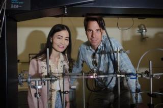 Nai-Chang Yeh and David Boyd. Credit: Lance Hayashida/Caltech Office of Strategic Communications
"With this new technique, we can grow large sheets of electronic-grade graphene in much less time and at much lower temperatures," says Caltech staff scientist David Boyd, who developed the method.
Graphene is an atom-thick layer of carbon having unique properties. It has electrical mobility that is many times better than silicon, and 200 times greater tensile strength when compared to steel. The measurement of the ease with which electrons can travel across the surface of a material is considered to be the electrical mobility.
Though achievement of these properties on an industrial scale has been desired, it has been complicated. In order to combine fabrication of graphene using the current electronic manufacturing processes, the required temperature is a very high 1800°F (1000°C). Furthermore, when graphene is grown at high-temperature, it causes deformation in the material which affects its intrinsic properties. The deformation is due to distributed, uncontrollable, large strain.
"Previously, people were only able to grow a few square millimeters of high-mobility graphene at a time, and it required very high temperatures, long periods of time, and many steps," says Caltech physics professor Nai-Chang Yeh, the Fletcher Jones Foundation Co-Director of the Kavli Nanoscience Institute and the corresponding author of the new study. "Our new method can consistently produce high-mobility and nearly strain-free graphene in a single step in just a few minutes without high temperature. We have created sample sizes of a few square centimeters, and since we think that our method is scalable, we believe that we can grow sheets that are up to several square inches or larger, paving the way to realistic large-scale applications."
In 2012, Boyd was a Caltech professor of mechanical engineering and applied physics. He was working in the late David Goodwin’s lab, and was attempting to create the same graphene-manufacturing process that he came to know about in a scientific journal. He used heated copper for catalyzing the graphene growth. "I was playing around with it on my lunch hour," says Boyd, who now works with Yeh's research group. "But the recipe wasn't working. It seemed like a very simple process. I even had better equipment than what was used in the original experiment, so it should have been easier for me."
When he was attempting this process, the phone rang and Boyd responded to the call. Meanwhile, he had left a copper foil to continue heating for a longer than desired period. This was before it got exposed to methane vapor, which provided the necessary carbon atoms required for growth of carbon.
Boyd used Raman spectroscopy to study the copper plate and he found that a layer of graphene had formed. "It was an 'A-ha!' moment," Boyd says. "I realized then that the trick to growth is to have a very clean surface, one without the copper oxide."
Nobel Prize–winning physicist Robert Millikan was the head of Caltech from 1921 to 1945. In 1916, he had conducted an experiment for measuring Planck's constant, and he had to contend with removal of copper oxide. This played an important role in calculating the energy contained in a photon or single particle of light. This inspired Boyd, and he contemplated whether it would be possible for him to work out a method for cleaning copper when it was under vacuum.
In the 1960s, a system was developed for generation of hydrogen plasma for removal of copper oxide at comparatively lower temperatures. Hydrogen plasma consists of hydrogen gas that has its electrons separated from the protons by electrification. Boyd utilized this idea in his experiments and found that the technique was able to remove the copper oxide, and also produce graphene. Initially, Boyd could not understand the success behind this technique. However, he found that very small amounts of methane were getting into the experiment chamber through two leaky valves. "The valves were letting in just the right amount of methane for graphene to grow," he says.
This method that enabled production of graphene without any active heating leads to a product with fewer defects, and lower manufacturing costs. Defects occur due to thermal contraction and expansion processes. Furthermore, this also does away with multiple post-production steps. "Typically, it takes about ten hours and nine to ten different steps to make a batch of high-mobility graphene using high-temperature growth methods," Yeh says. "Our process involves one step, and it takes five minutes."
A later study conducted by Yeh's group, along with international collaborators, demonstrated that graphene manufactured using the new process was of better quality when compared with graphene that was produced using traditional methods. Defects weaken the mechanical strength of graphene, and as this method delivers graphene with fewer defects, it has more strength. Furthermore, it has demonstrated very high electrical mobility for synthetic graphene.
The researchers consider that the efficiency behind their technique was a chemical reaction that took place between the air molecules and hydrogen plasma that led to generation of cyano radicals. These radicals are carbon-nitrogen molecules that have had their electrons removed. These are sort of tiny superscrubbers. They are charged molecules that clean the copper of the surface imperfections. This leads to a pristine surface for growth of graphene.
Graphene was also found to grow in a specific manner. When conventional thermal processes are used, graphene was found to grow from arbitrary patchwork of depositions. When the plasma technique is used, graphene grows uniformly. The graphene deposits initially form lines that grow to form a seamless sheet. This provides graphene with electrical and mechanical integrity.
“A scaled-up version of their plasma technique could open the door for new kinds of electronics manufacturing,” Yeh says. Graphene sheets that have low amount of defects could be utilized for protecting materials when exposed to the environment, and large sheets of graphene could be used in display panels and solar cells as transparent conducting electrodes. "In the future, you could have graphene-based cell-phone displays that generate their own power," Yeh says.
Yeh adds that intentional imperfections could be infused into the lattice structure of graphene so that they acquire specific electronic and mechanical characteristics. "If you can strain graphene by design at the nanoscale, you can artificially engineer its properties. But for this to work, you need to start with a perfectly smooth, strain-free sheet of graphene," Yeh says. "You can't do this if you have a sheet of graphene that has uncontrollable defects in different places."
Additional authors of this study include Wei Hsiang Lin, Chien-Chang Chen and Chen Chih Hsu, graduate students at Caltech; Marcus Teague, a staff scientist at Caltech; Yuan-Yen Lo, Chih-I Wu and Tsung-Chih Cheng of National Taiwan University; and Wen-Yuan Chan, Chia-Seng Chang, and Wei-Bing Su of the Institute of Physics, Academia Sinica.
The National Science Foundation, the Gordon and Betty Moore Foundation and the Kavli Foundation have provided funding support for this study. The Taiwanese National Science Council had supported the study in Taiwan.
The paper for this study titled "Single-Step Deposition of High-Mobility Graphene at Reduced Temperatures," has been published in the journal Nature Communications.