Jan 13 2016
A team of researchers, from the International Center for Materials Nanoarchitectonics of National Institute for Materials Science (NIMS) and the Georgia Institute of Technology, have developed a dual-layered nanowire that comprises a silicon (Si) shell and a germanium (Ge) core.
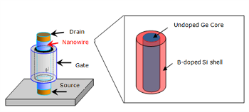 Schematic of a vertical transistor and an expanded view of its core-shell nanowire part.
The research group confirmed the functionalities of these stand-alone layers, as it was found that the carrier-transporting Ge layer and the impurity-doped Si layer were not intermixed. It was also discovered that carriers were produced in the Ge layer. Headed by principal investigator Naoki Fukata, the study shows that the innovative nanowire has the ability to suppress the impurity scattering, and is a potential candidate for next-generation transistor channels. Traditional nanowires tend to experience this impurity scattering.
Today, two-dimensional metal-oxide-semiconductor field-effect transistors (MOSFETs) are being used extensively, although attempts to miniaturize the MOSFET using traditional technology had reached it's limit. In order to resolve this problem a new method was proposed, this involved the development of a three-dimensional vertical transistor instead of a two-dimensional transistor. This approach could enable faster integration in comparison to standard transistors.
Semiconducting nanowires form the most critical component of the 3-D transistors, and researchers have proposed the use of these nanowires as channels. A major drawback of this approach is that in nanowires with a diameter of less than 20 nm, impurities doped into the nanowires to generate carriers cause the carriers to scatter, which reduced their mobility.
The researchers used the new nanowires, with the Ge core and Si shell, and produced high mobility channels. These nanowires can successfully isolate carrier transport regions from impurity-doped regions, and suppress impurity scattering. In addition, the team also validated the channels’ performance, carriers produced in the Si shell, are introduced into the Ge core of the nanowires.
Given that the mobility of carriers is relatively higher in the Ge layer in comparison to the Si layer, carrier mobility is significantly improved by the nanowire structure. Also, this structure inhibits the effect of surface scattering that can often occur in traditional nanowires. It was also demonstrated that the level of doping can control the carrier concentration.
Germanium and silicon are basic materials. Since these materials are required to produce the core-shell structure, nanowires can be developed at a relatively low cost. Future plans include using this core-shell structure to develop next-generation devices, whose performance and characteristics would be examined to evaluate their potential as high-speed devices.
This study was part of the research project and is titled “Control of Carrier Transport by Selective Doping of Core-Shell Heterojunction Nanowires”.
The NIMS 3rd Mid-Term Program project on chemical nanotechnology and the Japan Society for the Promotion of Science’s Grants-in-Aid for Scientific Research (A) program supported the study.