Apr 11 2016
The transistor is considered to be the most basic building blocks in the field of electronics, used to build circuits that can amplify electrical signals or switch them between the 0s and 1s at the heart digital computation. Transistor fabrication is an extremely complex process, which requires high-temperature, high-vacuum equipment.
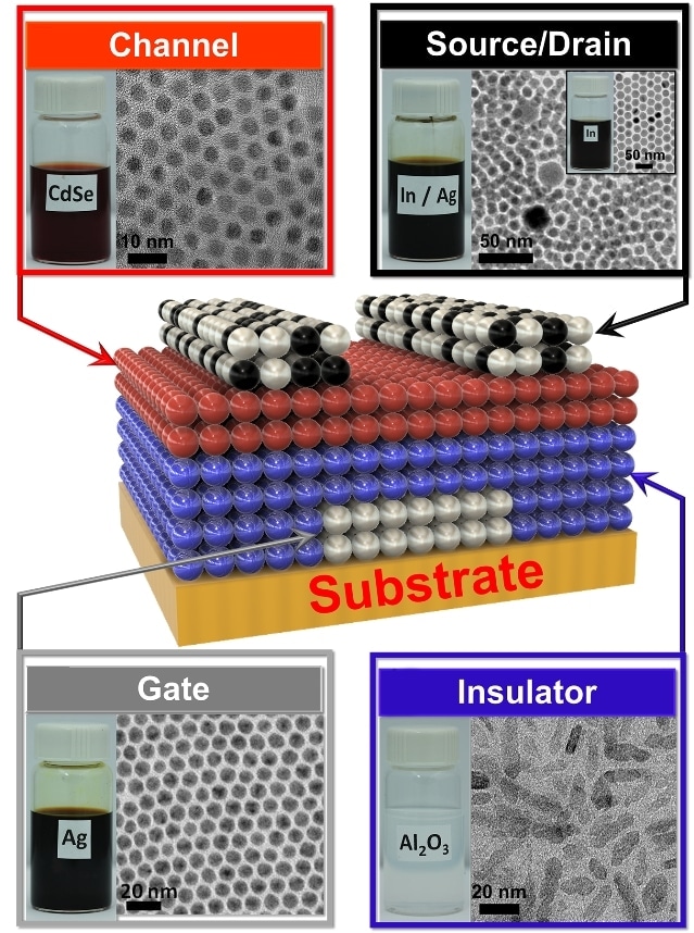 Kagan's group developed four nanocrystal inks that comprise the transistor, and then deposited them on a flexible backing.
Engineers from the University of Pennsylvania have discovered a new technique to build these devices: sequentially placing their components in the form of liquid nanocrystal “inks.”
The engineers have conducted a study on this new approach that has been published in Science. The study provides the potential for electrical components to be constructed into wearable and flexible applications, as the lower-temperature method is compatible with a variety of materials and can also be used for larger areas.
The nanocrystal-based field effect transistors were arranged on flexible plastic backings using spin coating, but could ultimately be built by additive manufacturing systems such as 3-D printers.
The study was headed by Cherie Kagan, the Stephen J. Angello Professor in the School of Engineering and Applied Science, and Ji-Hyuk Choi, then a member of her lab, now a senior researcher at the Korea Institute of Geoscience and Mineral Resources. Han Wang, Soong Ju Oh, Taejong Paik and Pil Sung Jo of the Kagan lab contributed to the work. They collaborated with Christopher Murray, a Penn Integrates Knowledge Professor with appointments in the School of Arts & Sciences and Penn Engineering; Murray lab members Xingchen Ye and Benjamin Diroll; and Jinwoo Sung of Korea’s Yonsei University.
Initially the researchers took roughly spherical-shaped nanoscale particles, or nanocrystals, with the electrical qualities essential for a transistor. They then dispersed these in a liquid, creating nanocrystal inks.
Kagan’s group created a library of four of the following inks, which include a conductor with a dopant (a mixture of indium and silver), a semiconductor (cadmium selenide), an insulator (aluminum oxide), and a conductor (silver). The process of doping the transistor’s semiconductor layer with impurities monitors whether the device transmits a negative or positive charge.
These materials are colloids just like the ink in your inkjet printer, but you can get all the characteristics that you want and expect from the analogous bulk materials, such as whether they’re conductors, semiconductors or insulators. Our question was whether you could lay them down on a surface in such a way that they work together to form functional transistors.
Cherie Kagan, Stephen J. Angello Professor, School of Engineering and Applied Science, University of Pennsylvania
The electrical properties of these nanocrystal inks have been separately examined, but they have never been incorporated into full devices.
This is the first work showing that all the components, the metallic, insulating, and semiconducting layers of the transistors, and even the doping of the semiconductor could be made from nanocrystals.
Ji-Hyuk Choi, Senior Researcher, Korea Institute of Geoscience and Mineral Resources
For this process, it is necessary to mix or layer them in accurate patterns.
Initially the conductive silver nanocrystal ink was introduced on a flexible plastic surface, treated with a photolithographic mask, and then swiftly spun to remove it in an even layer. The researchers then removed the mask so that the silver ink takes the shape of the gate electrode of the transistor. They followed that by spin-coating a layer made from aluminum oxide nanocrystal-based insulator. This was followed by spin-coating a layer of the cadmium selenide nanocrystal-based semiconductor, and finally a masked layer for the indium/silver mixture, which develops drain electrodes and the source of the transistor. After being heated at low temperatures, the indium dopant started to spread from those electrodes into the semiconductor component.
The trick with working with solution-based materials is making sure that, when you add the second layer, it doesn’t wash off the first, and so on. We had to treat the surfaces of the nanocrystals, both when they’re first in solution and after they’re deposited, to make sure they have the right electrical properties and that they stick together in the configuration we want.
Cherie Kagan, Stephen J. Angello Professor, School of Engineering and Applied Science, University of Pennsylvania
The ink-based fabrication process is carried out under lower temperatures in comparison to the existing vacuum-based methods, and because of this, the researchers were able to simultaneously construct a number of transistors on the same flexible plastic backing.
Making transistors over larger areas and at lower temperatures have been goals for an emerging class of technologies, when people think of the Internet of things, large area flexible electronics and wearable devices. We haven’t developed all of the necessary aspects so they could be printed yet, but because these materials are all solution-based, it demonstrates the promise of this materials class and sets the stage for additive manufacturing.
Cherie Kagan, Stephen J. Angello Professor, School of Engineering and Applied Science, University of Pennsylvania
The research was supported primarily by the National Science Foundation through its Materials Research Science and Engineering Centers Award DMR-1120901 and its Chemical, Bioengineering, Environmental, and Transport Systems Award CBET-1236406, the U.S. Department of Energy, Office of Basic Energy Sciences, Division of Materials Science and Engineering Award DE-SC0002158, the Office of Naval Research Multidisciplinary University Research Initiative Award ONR-N00014-10-1-0942, the Basic Research Project of the Korea Institute of Geoscience and Mineral Resources funded by the Ministry of Science, ICT and Future Planning of Korea.