Jun 13 2016
An international group of nanomaterials researchers from Korea University and the University of Illinois at Chicago (UIC) have developed a simple and affordable method to produce an ultrathin film, which is not only transparent, but also highly conductive to electric current.
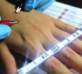 Highly conductive ultrathin film on skin between clips. Credit: SAM YOON/KOREA UNIVERSITY
The ultrathin film is a mat made of nanofiber and is electroplated to create a self-junctioned copper nano-chicken wire. It is also stretchable and flexible, offering the potential for use in different applications such as wearable electronics, roll-up touchscreen displays, electronic skin, and flexible solar. The research findings have been published in the June 13 issue of the journal, Advanced Materials.
It's important, but difficult, to make materials that are both transparent and conductive.
Alexander Yarin, Distinguished Professor of Mechanical Engineering, UIC
The new film establishes a "world-record combination of high transparency and low electrical resistance," the latter being at least 10-fold greater than the previous existing record, said Sam Yoon, who is also a corresponding author and a professor of mechanical engineering at Korea University.
The film also retains its properties after repeated cycles of severe stretching or bending, Yarin said – a critical property for wearables or touchscreens.
Manufacture begins by electrospinning a nanofiber mat of polyacrylonitrile, or PAN, whose fibers are about one-hundredth the diameter of a human hair. The fiber shoots out like a rapidly coiling noodle, which when deposited onto a surface intersects itself a million times, Yarin said.
The nanofiber spins out in a spiral cone, but forms fractal loops in flight. The loops have loops, so it gets very long and very thin.
Alexander Yarin, Distinguished Professor of Mechanical Engineering, UIC
Since the exposed PAN polymer does not conduct, it has to be spatter-coated with a metal in order to draw metal ions, and then the fiber is electroplated with copper, nickel, gold or silver.
According to the team, both the electroplating and electrospinning are comparatively high-throughput processes and can be commercially feasible processes, as they only take a few seconds to execute.
We can then take the metal-plated fibers and transfer to any surface -- the skin of the hand, a leaf, or glass.
Alexander Yarin, Distinguished Professor of Mechanical Engineering, UIC
A further application may be needed as a nano-textured surface that significantly increases the efficiency of cooling.
Yoon said the "self-fusion" by electroplating at the fiber junctions "dramatically reduced the contact resistance." Yarin also observed that the metal-plated junctions not only allowed percolation of the electric current, but also account for the physical resiliency of the nanomaterial.
"But most of it is holes," he said, which makes it 92% transparent. "You don't see it."
Source: http://www.uic.edu/