Jan 10 2020
Engineers from the University of California San Diego have developed a new technique that could allow fabrication of longer-lasting and more efficient perovskite solar cells, photodetectors, and LEDs.
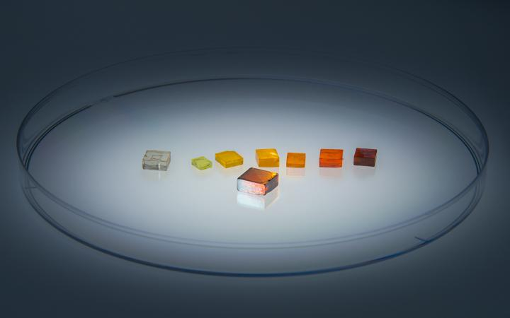 Strain-engineered, single crystal thin film of perovskite grown on a series of substrates with varying compositions and lattice sizes. Image Credit: David Baillot/UC San Diego Jacobs School of Engineering.
The researchers grew thin perovskite films on substrates with distinct compositions, offering a new method for fabricating perovskite single crystals with accurately deformed, or strained, structures.
The study was reported in the Nature journal on January 8th, 2020.
It is intriguing to engineer a small amount of strain in perovskites since it offers means to bring about considerable changes in the properties of the material, for example, the way it absorbs and transmits light, conducts electricity, or how stable it is.
You can use strain engineering as a knob to tune existing functions or even install new functions in a material.
Sheng Xu, Study Senior Author and Professor of Nanoengineering, Jacobs School of Engineering, UC San Diego
Although techniques are available that make use of heat to apply strain to perovskite crystals, that strain is usually short-lived or uncontrollable with respect to its magnitude. This fact renders the strain-engineered perovskites unfeasible to use. Moreover, current techniques for strain engineering are not compatible with device fabrication processes.
Xu and his colleagues dealt with these challenges by cautiously growing deformed perovskite single crystals. Their method involves permanently embedding strain into the structure of a material and enables them to customize the amount of strain—the extent of deformation of the crystal lattice is directly proportional to the strain.
Alpha-formamidinium lead iodide is the perovskite type analyzed in this research. This type has been employed to develop perovskite solar cells of highest efficiency to date. The team grew crystals of the material on a range of perovskite substrates with different lattice sizes and compositions—a process known as heteroepitaxial growth.
Upon being crystallized, the material adopted the lattice size of its substrate, which typically urged the alpha-formamidinium lead iodide crystals to grow in a different manner than they usually do.
Thus, the lattices in the material are deformed and strained to different degrees, depending on the lattice mismatch between material and substrate.
Yimu Chen, Study Co-First Author, Jacobs School of Engineering, UC San Diego
Chen is a nanoengineering PhD student in Xu’s lab.
“Because we are introducing strain at the atomic level, we can precisely design the strain and control it,” stated Yusheng Lei, who is the other co-first author of the study and also a nanoengineering PhD student in Xu’s lab.
The team grew perovskite crystals with five distinct strain levels ranging from 0% to −2.4%. It was found that samples with the optimal charge-carrier mobility were produced by a strain of −1.2%.
The team also reported another interesting discovery: growing alpha-formamidinium lead iodide crystals with strain stabilized its photoactive alpha phase.
In its strain-free form, alpha-formamidinium lead iodide undergoes a phase transition from a photoactive phase to a non-photoactive phase, which is bad for photovoltaic applications. With our growth method, we can lock the material’s crystal structure with that of the substrate to prevent this phase transition and enhance its phase stability.
Yimu Chen, Study Co-First Author, Jacobs School of Engineering, UC San Diego
As part of further research work, researchers will investigate the new functionalities and properties that can be strain-engineered into perovskites using their technique. They will also make efforts to scale up their method to grow large, single-crystalline thin films for industrial applications.
The co-authors of the study titled “Strain engineering and epitaxial stabilization of halide perovskites” include Yuheng Li, Yugang Yu, Jinze Cai, Yue Gu, Chunfeng Wang, Woojin Choi, Hongjie Hu, Chonghe Wang, Yang Li, Jiawei Song, Jingxin Zhang, Baiyan Qi, Muyang Lin, Zuorui Zhang, Shadi Dayeh, Kesong Yang, and Yu-Hwa Lo from UC San Diego; Ming-Hui Chiu and Lain-Jong Li from King Abdullah University of Science and Technology, Kingdom of Saudi Arabia; and Rahul Rao, Ahmad E. Islam, and Benji Maruyama from the Air Force Research Laboratory, Wright Patterson Air Force Base.
This study was supported by UC San Diego startup funds. This research was performed in part at the San Diego Nanotechnology Infrastructure (SDNI) at UC San Diego, a member of the National Nanotechnology Coordinated Infrastructure, which is supported by the National Science Foundation (grant ECCS-1542148).
Source: https://ucsd.edu/