Jul 1 2020
Graphene nanoribbons are the thickness of a single carbon atom as well as electrical properties that can exceed those of regular semiconductor technologies. These nanoribbons may lead to a new range of tiny electronic devices.
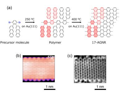 (a) Bottom-up synthesis scheme of 17-AGNR on Au(111), (b) high-resolution STM image, and (c) nc-AFM image of 17-AGNR. Image Credit: Junichi Yamaguchi, Yasunobu Sugimoto, Shintaro Sato, Hiroko Yamada.
But the concept continues to be far ahead of reality, considering the reduced potential of present-day graphene nanoribbons.
For the first time, a new collaborative study has reported a 17-carbon wide graphene nanoribbon, and effectively demonstrated that it has the tiniest bandgap observed so far among familiar graphene nanoribbons prepared through a bottom-up approach.
The study, published in the Communications Materials journal, is part of a project of CREST, JST Japan including Nara Institute of Science and Technology (NAIST), the University of Tokyo, and Fujitsu Laboratories Ltd and Fujitsu Ltd.
Silicon semiconductors are used by large-scale integrated circuits (LSIs). Such LSIs are employed in a variety of electronic devices, right from smartphones to computers. In fact, they are supporting people’s lives and virtually everything else nowadays.
But while LSIs have enhanced the performance of the devices by decreasing their size, LSI miniaturization is reaching its limits. Added to this, commercial demand also continues to place pressure on firms to develop smartphones that perform better at more compact sizes, whereas industry pressure is urging for commercial manufacturing with more miniaturized equipment.
According to group leader Dr Shintaro Sato from Fujitsu Ltd, other techniques and/or materials are certainly required to overcome these challenges.
Silicon semiconductors are giving us better performance at smaller sizes. However, we are reaching the limit in how small we can make devices. Thus, we have high expectations for the performance of graphene nanoribbons, which have semi-conducting properties that are only one atom thick—a 2D material.
Dr Shintaro Sato, Group Leader, Fujitsu Ltd
Graphene nanoribbons are essentially honeycomb-like structures and are less popular carbon-based semiconductor range when compared to carbon nanotubes and graphene. However, they have special magnetic and electronic properties that do not manifest in two-dimensional (2D) graphene.
Interestingly, the electronic and magnetic properties of graphene nanoribbons are widely tuned as a function of the width and edge structure.
Hiroko Yamada, Professor, Nara Institute of Science and Technology
Furthermore, width-dependent bandgap is present in armchair-type graphene nanoribbons, which are a potential type of nanoribbon intended for device application. These graphene nanoribbons can be categorized into three subfamilies—that is, 3p, 3p + 1, and 3p + 2—since their bandgaps are inversely proportional to the thickness of those families.
Fundamentally, broader armchair-edge graphene nanoribbons, which are part of the 3p + 2 subfamily, exhibit the tiniest bandgaps among varying types of graphene nanoribbons. These nanoribbons could be considerably manipulated in GNR-based devices.
To date, researchers have reported 13-armchair graphene nanoribbons that belong to the 3p + 1 subfamily with a bandgap of over 1 eV; however, Sato, Yamada, and their collaborators have demonstrated the production of a 17-graphene nanoribbon that belongs to the 3p + 2 subfamily and displays even smaller bandgaps.
The development of this graphene nanoribbon was based on the bottom-up method, known as “on-surface synthesis.” A dibromobenzene-based molecule was also employed as a precursor for producing on-surface graphene nanoribbons.
There are many methods to synthesize graphene nanoribbons, but to produce atomically precise graphene nanoribbons, we decided to use the bottom-up approach. The important point is that the structure of the precursor can define the ultimate structure of graphene nanoribbons if we use the bottom-up approach.
Dr Hironobu Hayashi, Nara Institute of Science and Technology
Dr Hayashi also contributed to the research.
Scanning tunnel spectroscopy and microscopy performed by Dr Junichi Yamaguchi from Fujitsu Ltd as well as non-contact atomic force microscopy conducted by Dr Akitoshi Shiotari and Professor Yoshiaki Sugimoto from The University of Tokyo demonstrated the atomic and electronic structure of the resultant 17-armchair graphene nanoribbons.
The bandgap of 17-armchair graphene nanoribbons, which was acquired experimentally, was also found to have a bandgap of 0.6 eV. This is the first-ever demonstration of the development of graphene nanoribbons that have a bandgap smaller than 1 eV in a regulated way.
“We expect these 17-carbon wide graphene nanoribbons to pave the way for new GNR-based electronic devices,” concluded Sato.
Journal Reference:
Yamaguchi, J., et al. (2020) Small bandgap in atomically precise 17-atom-wide armchair-edged graphene nanoribbons. Communications Materials. doi.org/10.1038/s43246-020-0039-9.
Source: http://www.naist.jp/en/