Ferroelectric materials feature special inner structures. Regarding the crystalline materials, the ions organize themselves distinctly within individual areas known as the domains. Electric field or external pressure can be employed to change the so-called polarization.
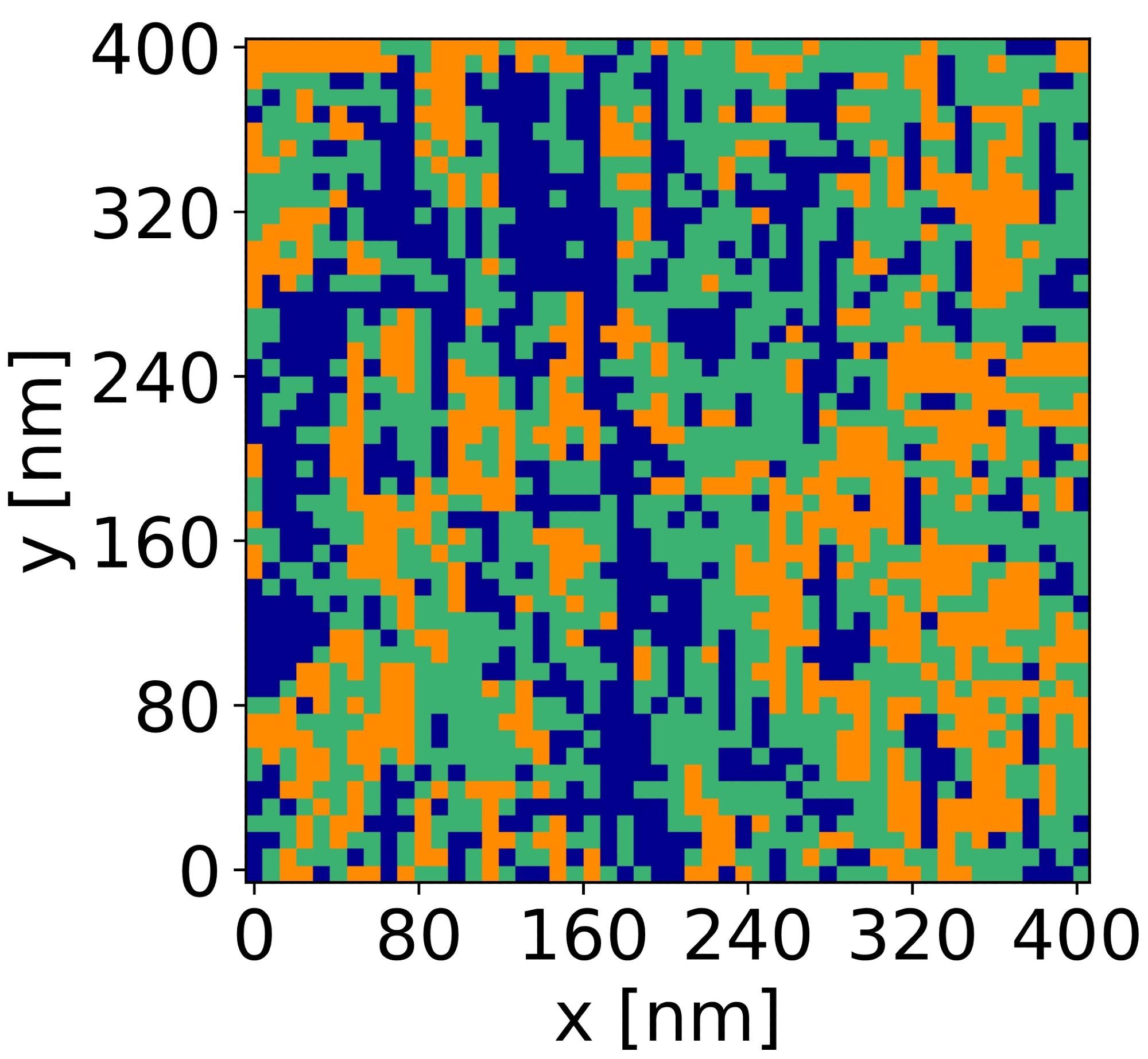 Map obtained for a thin barium titanate film after clustering the data measured by contact Kelvin probe force microscopy (cKPFM) by a machine learning method. From this map, scientists can obtain detailed information on how the ferroelectric domains are distributed and what their respective polarization amplitude is. Image Credit: Helmholtz Zentrum Berlin für Materialien und Energie.
These characteristics make ferroelectric materials unique for several technical applications. For example, they are ideal as a material for capacitors — or, due to the domains being very small, for the storage of a large amount of data in a small space.
However, what makes the ferroelectric properties change when the material’s dimensions are significantly decreased, for example, to employ them in nanoelectronic parts? Experiments have demonstrated that shrinking has a huge effect on the pattern of ferroelectric polarization.
When the dimensions are reduced, the ferroelectric domains can take on a very different shape with a spatial extension of only several nanometers. The diversity of electrical structures on a nanocrystalline scale opens up a whole new exciting horizon both for the understanding of the physics of these objects and for their potential applications. One key challenge is to be able to visualize such tiny domains in a non-destructive way.
Dr. Catherine Dubourdieu, Professor and Head, Institute Functional Oxides for Energy Efficient IT, Helmholtz Zentrum Berlin für Materialien und Energie
Catherine Dubourdieu and her team together with other researchers at the Oak Ridge National Laboratory (ORNL) in the United States have now discovered an approach to map the polarization pattern in thin ferroelectric layers accurately and non-destructively. For this purpose, the researchers depended on the so-called contact Kelvin probe force microscope (cKPFM), a technique that calculates the electromechanical response of the material under an electrical bias.
The HZB team employed a machine learning technique to analyze the huge amount of data generated by mapping as low as 8x8 nm2 pixel size. This made it palpable to spatially resolve the ferroelectric domains of less than 10 nm in size and of different polarization amplitudes.
The research team used titanate (BaTiO3) in two crystalline forms as sample material. The first was in the so-called called perovskite structure (one of the well-known ferroelectric materials) and the second in the hexagonal structure, which is not ferroelectric at ambient temperature.
To verify the dependability of the measurement technique employed, the HZB and ORNL teams also tested the nanostructures using a transmission electron microscope (TEM).
Dubourdieu said, “The results of both experimental methods were in complete agreement.” It was also possible for the scientists to use this technique to follow the ferroelectric pattern evolution during the heating of the sample to its paraelectric state. This creates the opportunity to investigate the temperature reliance of the ferroelectric domain distribution and observe the way in which ferroelectric domains form spatially below the so-called Curie temperature.
Our results create a promising new perspective to study a large variety of polarization patterns at the nanoscale. This could lead, for example, to mapping the distribution of topological polar textures such as polar skyrmions which have been shown to have dimensions of about 10 nm. It could also be used to discriminate the polar domains from the non-polar ones in polycrystalline HfO2-based ferroelectric thin films, a type of materials intensively studied for their potential integration in current nanoelectronics.
Dr. Catherine Dubourdieu, Professor and Head, Institute Functional Oxides for Energy Efficient IT, Helmholtz Zentrum Berlin für Materialien und Energie
“In the future, mapping ferroelectricity at the nanoscale with the help of machine learning will undoubtedly bring insights into phenomena occurring when dimensions are reduced and bring benefit for the integration of ferroelectrics into nanodevices,” concluded Dubourdieu.
Journal Reference:
Schmitt, S. W., et al. (2021) Sub-10 nm Probing of Ferroelectricity in Heterogeneous Materials by Machine Learning Enabled Contact Kelvin Probe Force Microscopy. ACS Applied Electronic Materials. doi.org/10.1021/acsaelm.1c00569.
Source: https://www.helmholtz.de/en/