A group of researchers recently published a paper in the journal Nature Communications that demonstrated the effectiveness of atomic level height steps in strongly scattering the mid-infrared acoustic graphene plasmons (AGPs).

Study: Strong in-plane scattering of acoustic graphene plasmons by surface atomic steps. Image Credit: sakkmesterke/Shutterstock.com
The Benefits of Graphene Plasmons
GPs-electromagnetic fields linked with charge carrier oscillations have gained considerable prominence due to their unique properties, such as electric tunability, robust field confinement, and short wavelengths.
These properties make GPs a suitable choice for controlling electromagnetic waves at the nanometer scale in different applications such as highly integrated sensitive modulators and detectors.
The GPs can hybridize with their mirror image and form an electromagnetic mode comprised of anti-phase charge oscillations in the metal and the graphene when the graphene sheet is placed on a metallic surface. This new hybridized electromagnetic mode that satisfies the momentum versus linear energy dispersion is referred to as AGPs.
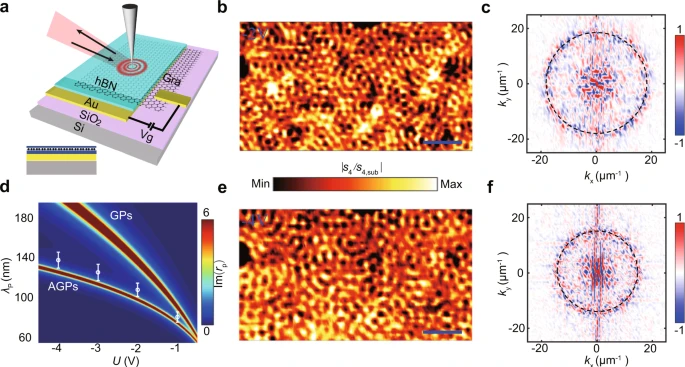
Figure 1. Structure and the near-field response of an acoustic graphene plasmon (AGP) device. a Schematic of the AGP device, which is composed of h-BN (2 nm)/graphene/h-BN (6 nm) heterostructure placed on Au (50 nm)/SiO2 (300 nm)/Si substrate. The inset shows the cross-section view of the AGP device. b Real space near-field image of the AGPs at −2 V, the color bar represents the normalized intensity. c The amplitude of the Fourier transformation of (b) in momentum space (kx, ky). d The comparison between the wavelength and back gate voltage-dependent dispersion of AGPs and that of graphene plasmons (GPs). The dispersion was obtained by caculating the imaginary of the reflection coefficient (Im(rp)) with the transfer matrix method. The white circles represent the experimental results. The error bars show the width of the concentric circles in momentum space. e, f Near-field image of the AGPs at −4 V and the corresponding Fourier transform. The wavelength of excitation light is λ = 10.653 μm. Scale bars, 300 nm. © Zhang, N., Luo, W., Wang, L. et al. (2022)
AGPs often lead to ultra-strong enhanced and confined electric fields within the gap between the two materials. These fields can be extensively confined in-plane to almost 1/300 of their corresponding free-space wavelength.
Additionally, AGPs can assist in exploring the quantum effects owing to their ability of plasmon confinement at the atomic level, while the AGP-provided field concentration can improve the infrared molecular vibrational spectroscopy sensitivity in ångström-thick material layers.
Currently, far-field infrared spectrum and near-field photocurrent nanoscopy are used to explore the AGP properties in the infrared or THz ranges as direct detection of infrared near-field optical scattering is still extremely challenging, specifically the in-plane scattering properties of AGPs. However, in-plane scattering properties are essential for the utilization and manipulation of ultraconfined optical fields at the atomic level.
In this study, researchers deposited mid-infrared AGPs modes in hexagonal boron nitride (h-BN) encapsulated graphene on the top of an Au surface. The thickness of the atomic level steps were analyzed using scattering-type scanning near-field optical microscopy (s-SNOM).
Fabricating the Heterostructures
s-SNOM imaging of the AGP in-plane scattering was performed. The heterostructure devices used in the experiment comprised a monolayer graphene flake that was encapsulated between two layers of h-BN.
The polymer-free van der Waals assembly technique was used to fabricate the h-BN (6 nm)/graphene/hBN (2 nm) heterostructure. s-SNOM based on metallic atomic force microscopy (AFM) tip was employed to perform the near-field imaging. A 10.653 μm infrared laser was focused on the AFM tip.
The fabricated heterostructure was placed on the top of the 50 nm Au gate, where the h-BN layer at the bottom of the heterostructure acted as a spacer, and GPs were proposed to hybridize with their mirror image and form AGPs.
The propagating AGPs in the heterostructure devices were visualized at room temperature by infrared nano-imaging at back-gate voltages of -4 and -2, respectively.
The gold (Au) substrate and the encapsulated sample topography were analyzed to identify the scattering sources. Energy-dispersive X-ray spectroscopy (EDS) and scanning electron microscope (SEM) were employed to characterize the sample atomic composition.
A theoretical two-dimensional (2D) model was adopted to determine the reason behind the strong backscattering of AGPs at such shallow steps of 3 nm on the Au substrate. Another sample with spatially separated scatterers was studied to determine the scattering behavior of the individual scatterers.
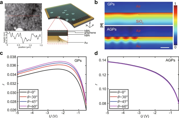
Figure 2. The advantage of in-plane reflectivity of mid-infrared acoustic graphene plasmons (AGPs) compared to graphene plasmons (GPs). a Schematic diagram of the simplified calculation model. The left panels show the AFM topography of the h-BN/graphene/h-BN heterostructure placed on the gold surface, where a fluctuation in a depth of about 3 nm exists. Deduced from the topographic differences between the sample and bare gold substrate, the height of the reflection boundaries is set as 3 nm. The angle θ is the angle between the surface normal and the tangent of boundary on the left side of hole. b The magnetic field profile of ∣H∣ during reflection at θ = 0∘ for GPs and AGPs. Scale bar, 30 nm. c, d Show back gate voltage U dependent reflectivity r of GPs and AGPs for different steepness of steps, respectively. © Zhang, N., Luo, W., Wang, L. et al. (2022)
Observations
A sharp tip apex provided the wave vector matching between incident photons and plasmons, where a part of incident light is converted to plasmons.
The interference between plasmon waves and the incident light reflected from graphene edges led to the creation of fringes. The period of fringes was one-half of the polariton wavelength.
Plasmon interference fringes were observed in the AGPs at room temperature for the first time. The fringes generated from the collective plasmon scattering by several scatterers, and were distributed in a disordered manner and varied substantially at various gate voltages.
Randomly distributed holes were observed on the uncovered Au surface with around 6 nm depths. Similar-shaped holes were also observed in the sample with shallower depths, which indicated a suspended device on the uneven Au substrate.
The holes formed by the Au substrate were identified as scattering sources for the plasmon fringes. Additionally, the AFM topography of the samples and surrounding nano-fields confirmed the role of Au substrate as scattering sources.
Images obtained from the Fourier-transformed near-fields also demonstrated that AGPs acted as the source of the plasmon interference fringes.
The AGP dissipation depended on the gate voltage as the voltage influenced the dissipation time. The atomic-level height steps strongly scattered the mid-infrared AGPs even when the scatterer step height was four orders of magnitude smaller compared to the incident-free wavelength, indicating larger backscattering of AGPs compared to conventional GPs.
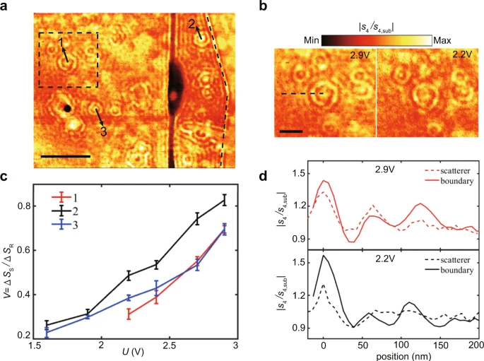
Figure 3. The near-field response of individual scatterers at the wavelength of λ = 10.653 μm. a The near-field image of the sample region over a 2.6 μm × 2 μm area under the gate voltage of 2.9 V. The black dashed line and rectangle show the boundary and the selected scatterer area of the h-BN encapsulated single-layer graphene, respectively. Three obvious isolated scatterers are labeled as 1, 2, and 3 by arrows. Scale bar, 500 nm. b Near-field images of the acoustic graphene plasmons (AGPs) in the region of the black dashed square in (a) (the scatterer 1) at 2.9 and 2.2 V, respectively. The black dashed line represents the position where the detailed near-field closed to the scatterer is investigated in (d). Scale bar, 300 nm. c The fringe visibility (V) for the three different scatterers as a function of the gate voltages U. The errors bars show the fluctuation of ΔSS/ΔSR in different azimuthal directions close to the scatterers. d Comparison between the normalized near-field signal S4/S4,sub of the selected scatterer and the boundary of the graphene as a function of the voltages. The dashed and solid lines represent the scatterer and the boundary, respectively. © Zhang, N., Luo, W., Wang, L. et al. (2022)
The reflectivity was 13% for AGPs and 3.8% for GPS at a shallow depth of 3 nm owing to the larger vertical field localization between the graphene and metal gap for AGPs compared to GPs.
A large reflection of AGPs was observed at the nanometer scale without requiring any incontinuity of the electronic conductivity of graphene.
The AGP scattering by the individual scatterers was controlled through electrical back gating.
To summarize, the findings of this study presented a viable way to control ultraconfined optical fields with atomic-level height steps.
Reference
Zhang, N., Luo, W., Wang, L. et al. (2022) Strong in-plane scattering of acoustic graphene plasmons by surface atomic steps. Nature Communications https://www.nature.com/articles/s41467-022-28614-z
Disclaimer: The views expressed here are those of the author expressed in their private capacity and do not necessarily represent the views of AZoM.com Limited T/A AZoNetwork the owner and operator of this website. This disclaimer forms part of the Terms and conditions of use of this website.