In a study published in the journal Light: Science & Applications, to optimize the carrier content and transportation, a desorption customizing technique was developed, and self-arranged p-AlGaN superlattices having a mean aluminum content of more than 50 percent were created.
Study: Sub-nanometer ultrathin epitaxy of AlGaN and its application in efficient doping. Image Credit: Gorodenkoff/Shutterstock.com
The Problem of Doping Asymmetry in Semiconductors
Semiconductive materials are at the core of present optoelectronic and electronic devices, thanks to the advent of regulated doping methods. Whilst certain devices may be constructed using monopolar conduction, most rely on good n-type and p-type doping. However, semiconductors, particularly wide-gap semiconductors, have an inherent doping asymmetric problem, in which one form of dopant is relatively easy to obtain while the other has proven to be a huge obstacle.
Considering ZnO and AlGaN, for instance, they possess desirable n-type conductance; however, achieving p-type conductance is very difficult due to their valence bands being somewhat distant from the vacuum level. In the case of diamonds, the situation is reversed.
The problem of asymmetric loading greatly limits the production of technologies, generally deep-UV optoelectronic gadgets based on AlGaN, due to a scarcity of good aluminum-rich p-AlGaN.
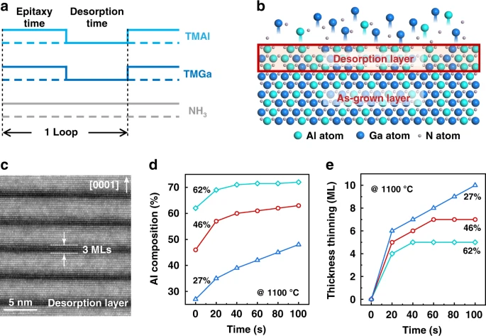
Figure 1. Schematic process and corresponding structural features of the interrupted epitaxy. a Schematic process of the periodically interrupted epitaxy. b Schematic illustration of the self-assembled bilayer structure by desorption-tailoring. c Z-contrast image of the self-assembled bilayer structures in AlGaN with the desorption time and initial Al composition of 80 s (at 1100 °C) and 46%, respectively. d Desorption time dependence of Al composition in the desorption layer. e Desorption time dependence of the thinning thickness in the as-grown layer. © Wang, J., Wang, M. et al. (2022).
Critical Factors in Resolving the Doping Asymmetry Issue
When trying to tackle the loading problem, carrier content and transportation must be balanced. With respect to carrier density, numerous possibilities must be addressed, such as dopant solubility, where the dopants lie on the lattice locations, activating energy of the dopants, and self-compensation via internal imperfections.
In terms of carrier transportation, emphasis should be placed on meeting the need for carrier insertion in device applications. Considering aluminum-rich p-AlGaN, for instance, while Mg is proven to be a moderately effective p-type dopant, the fundamental challenges continue, namely unusually large acceptor activating energy and rather poor Mg solubility.
An activating energy of more than 300 meV may be predicted in aluminum-rich (more than 50 percent) AlGaN, which is significantly more than the heat energy at ambient conditions, leading to an exceptionally poor activating efficiency of Mg. Even worse, because of the positive and high synthesis enthalpies, Mg's solubility as a replacement for Ga or Al in AlGaN is relatively restricted.
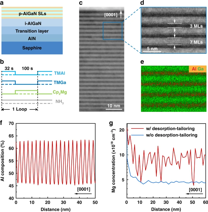
Figure 2. Preparation of Al-rich p-AlGaN SLs by adopting the desorption-tailoring strategy. a Schematic illustration of the sample with desorption-tailored p-AlGaN SLs. b Schematic process of desorption-tailoring for p-AlGaN SLs. c HRTEM image of the p-AlGaN SLs. d Z-contrast image of the p-AlGaN SLs. e Distribution of Al and Ga atoms by EDS mapping corresponding to the region in panel d. f EDS line scanning curve of Al composition in the p-AlGaN SLs. g Mg concentration profile by SIMS in the desorption-tailored p-AlGaN SLs as well as in an uninterrupted-grown Al0.63Ga0.37N epilayer (without desorption-tailoring). © Wang, J., Wang, M. et al. (2022).
Different Approaches of Addressing the Issue
Owing to the various challenges, the hole content in aluminum-rich p-AlGaN is very low, far from meeting product requirements.
A variety of focused techniques have been presented thus far, such as superlattice (SL) dopants, loading with quantum-dots, and polarization-triggered loading for lowering Mg activating energy threshold; delta doping and enhanced surface architecture for increasing Mg integration, and so on. Despite the fact that various methodologies have been used to construct similar gadgets, a comprehensive strategy for p-type loading in aluminum-rich AlGaN is yet to be established.
Most techniques fail to address all of the issues highlighted above and may even have a detrimental impact on certain elements while addressing others. For instance, superlattice loading significantly decreases activating energy by changing the band configuration, nevertheless, vertical hole transportation is often obstructed by obstacles, especially because super-thin (less than 1 nm) ternary AlGaN is hard to manufacture consistently.
Likewise, enhanced surface architecture improves Mg integration into AlGaN by producing optimal N-rich settings, but the problem of high activating energy continues. Thus, an all-encompassing strategy for resolving the p-doping problem in aluminum-rich AlGaN is eagerly anticipated.
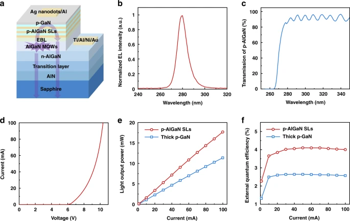
Figure 3. Performance of DUV-LEDs fabricated with desorption-tailored Al-rich p-AlGaN SLs. a Schematic illustration of DUV-LEDs with desorption-tailored p-AlGaN SLs. b EL spectrum (at 100 mA) of DUV-LEDs. c Transmission spectrum of the desorption-tailored p-AlGaN SLs (without the p-GaN contact layer). d I–V curve of DUV-LEDs with the p-electrode of complex Ag nanodots/Al. e, f Dependence of the LOP and EQE on the injection current for DUV-LEDs with desorption-tailored p-AlGaN SLs and thick p-GaN, respectively. © Wang, J., Wang, M. et al. (2022).
Key Findings of the Study
In this paper, a desorption-adjusting technique was offered to solve the significant problem of asymmetric loading, which involves optimizing carrier density and transportation. When applied to p-AlGaN, self-arranged p-AlGaN superlattices with a mean aluminum content of 51 percent were created.
Large hole content was achieved at ambient conditions due to a large decrease in the acceptor activating energy threshold along with a marked increase in Mg surface-integration. Furthermore, the vertical miniband transportation of holes in the p-AlGaN superlattices was proven, considerably answering the requirement for hole insertion in systems, thanks to the consistent super-thin barrier width in this strategy.
As an example, 280 nm DUV-LEDs were made using desorption optimized aluminum-rich p-AlGaN superlattices, resulting in a 55 percent improvement in light output power (LOP). This work is intended to give a strategy for p-type loading in aluminum-rich AlGaN, as well as to offer insight on how to solve the asymmetric loading problem in general for wide-gap semiconductors, particularly ternary and quaternary compound semiconductors.
Reference
Wang, J., Wang, M. et al. (2022). Sub-nanometer ultrathin epitaxy of AlGaN and its application in efficient doping. Light: Science & Applications, 11. Available at: https://www.nature.com/articles/s41377-022-00753-4
Disclaimer: The views expressed here are those of the author expressed in their private capacity and do not necessarily represent the views of AZoM.com Limited T/A AZoNetwork the owner and operator of this website. This disclaimer forms part of the Terms and conditions of use of this website.