Since its discovery in 2004, graphene has been praised as a wonder material of the future. The ultrathin carbon material is an extremely strong thermal and electrical conductor, making it an ideal component to improve semiconductor chips employed in numerous electrical gadgets.
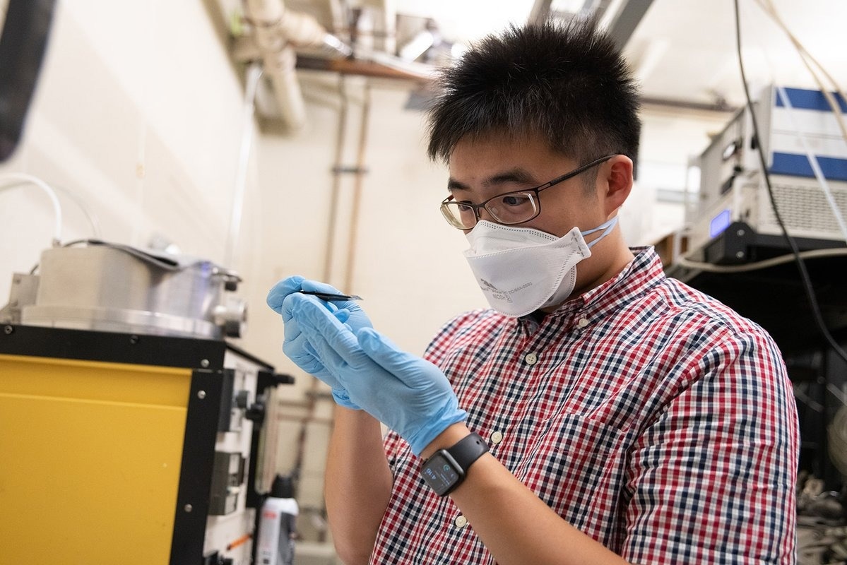
Chen-Hsuan (Steve) Lu inspects a substrate coated in graphene. Image Credit: Caltech
Although graphene-based studies have accelerated, the nanomaterial has not been able to progress as rapidly: specifically, manufacturers are not able to produce large, industrially applicable quantities of the material.
A new study from the lab of Nai-Chang Yeh, the Thomas W. Hogan Professor of Physics, is bolstering the graphene trend.
In two recent studies, scientists show that graphene can significantly enhance electrical circuits needed for wearable and flexible electronics like smart health patches, bendable smartphones, helmets, large folding display screens, and more.
In one study reported in ACS Applied Materials & Interfaces, the scientists grew graphene straight onto thin two-dimensional (2D) copper lines usually used in electronics. The findings revealed that the graphene-enhanced the lines' conducting features as well as safeguard the copper-based structures against standard wear and tear.
For example, they demonstrated that graphene-coated copper structures could be folded 200,000 times without any deformation, as compared to original copper structures, which began cracking after 20,000 folds. The findings revealed that graphene could help form bendable electronics with longer service life.
The second study, reported in the journal ACS Applied Nano Materials, showed that gold coated in graphene could better endure the sweat of an individual's body, and can be utilized to build improved implantable biosensors.
Gold is a typical component used in creating implantable biosensors or smart patches—nanoscale tools for tracking numerous health conditions. Graphene decelerated the rate at which the gold oxidizes.
A third study reported in the journal ACS Applied Materials & Interfaces demonstrated that graphene could safeguard electrical circuits formed via inkjet printers. They used the team’s exclusive technique for growing graphene.
In 2015, Yeh and her contemporaries, including Senior Research Scientist David Boyd, claimed that they had found a better, more economical, and eco-friendly way to grow graphene on materials.
The technique referred to as plasma-enhanced chemical vapor deposition can be employed to grow superior quality graphene sheets, just one atom in thickness, at room temperature in approximately 15 minutes. This is in contrast to other approaches that necessitate harsh chemicals, much higher temperatures, and require many hours to complete.
Flexible and wearable electronics can be made of soft materials like polymers that can't sustain high temperatures. Our method allows us to grow graphene directly on the substrates at a low temperature, preventing any damage to sensitive materials.
Chen-Hsuan (Steve) Lu (MS '20), Study Lead Author and Graduate Student, Caltech
Yeh explains that their graphene-growth technique, which can be expanded to suit industrial requirements, is well-matched with a range of other applications besides bendable and wearable electronics.
Our method is highly compatible with all kinds of substrates, ranging from tiny, nanostructure metals, to semiconducting materials, to even plastics. Because we don't require high temperatures, this method can be used on different substrates for many applications.
Nai-Chang Yeh, Thomas W. Hogan Professor, Physics, Caltech
Pink Plasma
The team’s technique for growing sheets of graphene was conducted in their basement lab. A ray of plasma that glows pink in color is employed to trigger a gas of methane and hydrogen molecules and break them down into smaller bits.
The sample, such as a 2D copper line, is soaked in the plasma, and the carbon from the gas is deposited onto the surface in thin sheets that are one atom in thickness. The final surface containing the graphene will look shinier.
“Because the sample is immersed in the plasma without the need of active heating up to about 1,000 degrees Celsius by a hot furnace, which is the case with other methods, much lower-temperature growth becomes feasible,” Lu says.
For the research where the ability of graphene to improve the flexibility of electronics was tested, the team collaborated with the Materials and Chemical Research Laboratories at the Taiwanese organization called Industrial Technology Research Institute (ITRI).
The Caltech group developed graphene-coated copper structures that imitate what would be used in bendable electronics and then had their colleagues at ITRI fold them; the company has the equipment needed to continually fold the structures hundreds of thousands of times.
“I tried and was not able to stand there and fold the materials this long myself,” Lu jokes.
The ITRI has been playing an important role in bridging laboratory research to industrial productions in Taiwan over decades. The most well-known example among many spin-off companies from ITRI is the Taiwan Semiconductor Manufacturing Company (TSMC), currently the world's largest and leading semiconductor foundry.
Nai-Chang Yeh, Thomas W. Hogan Professor, Physics, Caltech
In this same research, the scientists also demonstrated that graphene could enhance the electrical conductivity and chemical stability of copper structures, besides their structural flexibility.
“We put just two atomic layers of graphene on top of these thin copper lines and saw that they were beautifully unchanged after several months,” Yeh says.
The second study verified whether graphene could safeguard the durability of gold structures employed in implantable biosensors. The team grew graphene on gold and then placed the material in saline liquid to simulate sweat.
The outcomes revealed that the graphene-coated structure stayed intact under conditions corresponding to around one month at regular human body temperatures, a lot longer than what is achievable with just gold.
I wasn't aware of graphene’s full potential when I first started working with it. But then I realized how it can be used in tandem with other materials for so many applications. My roommate [co-author Kuang Ming (Allen) Shang] and I were having a boba tea when we realized we could test whether graphene might protect gold from the corrosive effects of sweat.
Chen-Hsuan (Steve) Lu (MS '20), Study Lead Author and Graduate Student, Caltech
What is Next for Graphene?
Although graphene has taken a lot of time to enter into electronics than first predicted, its future seems bright. Besides graphene applications in wearable and bendable electronics, Yeh is scrutinizing graphene’s potential in everything from optical communications and energy research to eco-friendly batteries and more.
Furthermore, Yeh adds that graphene is paramount to the growing domain of nanoelectronics, which aims to develop smaller models of the electronics extensively used at present. Graphene can be employed along with silicon to shrink devices down to extremely smaller sizes.
“Graphene, when combined with other materials, can make our nanotechnologies smaller and faster. It leads to lower heat dissipation and energy consumption. In our lab, we use graphene for so many things. It’s exciting,” she says.
New Graphene Method to Protect and Enhance Biomedical Devices
Video Credit: Caltech
Journal References
- Lu, C-H., et al. (2022) Polymer-Compatible Low-Temperature Plasma-Enhanced Chemical Vapor Deposition of Graphene on Electroplated Cu for Flexible Hybrid Electronics. ACS Applied Materials & Interfaces. doi.org/10.1021/acsami.1c11510.
- Lu, C-H., et al. (2022) Graphene on Nanoscale-Thick Au Films: Implications for Anticorrosion in Smart Wearable Electronics. ACS Applied Nano Materials. doi.org/10.1021/acsanm.2c00401.
- Lu, C-H., et al. (2022) Single-Step Direct Growth of Graphene on Cu Ink toward Flexible Hybrid Electronic Applications by Plasma-Enhanced Chemical Vapor Deposition. ACS Applied Materials & Interfaces. doi.org/10.1021/acsami.0c22207.
Source: https://www.caltech.edu