Flakes of two-dimensional (2D) materials have exceptional quantum qualities that are not seen in common materials since they only have one to a few atomic layers. As a result, these materials have a tremendous amount of potential for both advanced research and industrial applications.
TOC image. Image Credit: Hebrew University of Jerusalem/ACS Publications
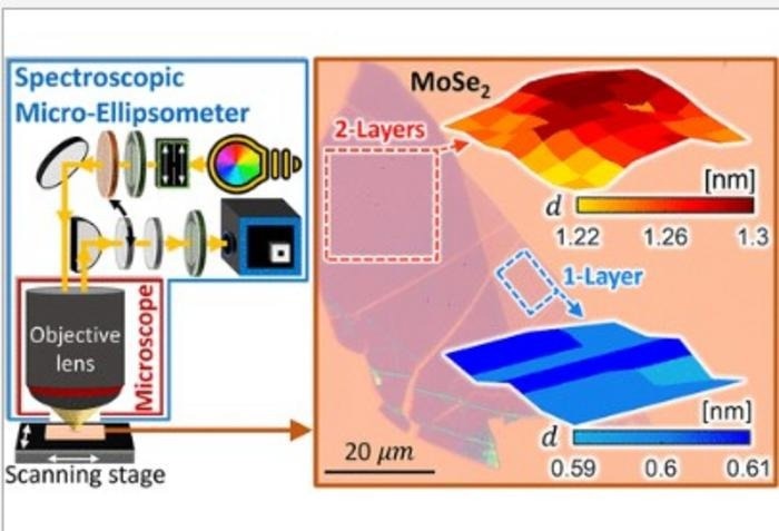
In the past, ellipsometry has been a commonly used optical method for noninvasive measurement of thin-film thicknesses. Commercial ellipsometers, on the other hand, have difficulties when it comes to measuring regions that are smaller than 50–60 microns, while 2D flakes frequently only have lateral dimensions of a few microns.
Spectroscopic Micro-Ellipsometer (SME), a system and method for a microscope-integrated ellipsometer, was created and patented by Prof. Ronen Rapaport and Ralfy Kenaz of Hebrew University in response to this substantial challenge.
With this state-of-the-art tool, thin-film thickness measurements in incredibly small areas—down to just 2 microns wide—can be made quickly and with atomic-level accuracy. The instrument's outstanding performance has already been confirmed in a different publication, enhancing its legitimacy and dependability.
Researchers from Hebrew University used this cutting-edge micro-ellipsometer to address the current scientific challenge of measuring and mapping the thicknesses of atomically thin 2D material flakes in a new study published in the journal ACS Nano.
The results clearly show that the micro-ellipsometer can measure and map the thicknesses of various 2D material flakes, enabling the estimation of their atomic layer count.
The results of this study have broad ramifications for a variety of microstructure-related companies and research domains. They pave the way for extremely precise optical studies of microstructures, which will lead to technological improvements and new horizons in science.
This research delivers a fresh and priceless system for both researchers and companies by introducing the application of the well-established and extremely sensitive ellipsometry technique to microstructures.
There are numerous possible uses for the Spectroscopic Micro-Ellipsometer in the thin film industry, including quality control of wafers, characterizing 2D devices and nanoscale metamaterials, and examining the crystal structure of nanoparticles.
Prof. Hadar Steinberg’s lab, also from the Racah Institute of Physics at Hebrew University, specializing in the study of 2D materials, worked closely with Prof. Ronen Rapaport’s lab from the Racah Institute of Physics, known for their proficiency in optics investigations.
Journal Reference
Kenaz, R., et al. (2023) Thickness Mapping and Layer Number Identification of Exfoliated van der Waals Materials by Fourier Imaging Micro-Ellipsometry. ACS Nano. doi:10.1021/acsnano.2c12773.
Source: https://en.huji.ac.il/